

High strip rate downstream chamber
a downstream chamber and high strip rate technology, applied in the field of wafer processing, can solve the problems of back pressure, slow down the gas flow above the showerhead, and reduce the effect of flow dynamics
- Summary
- Abstract
- Description
- Claims
- Application Information
AI Technical Summary
Benefits of technology
Problems solved by technology
Method used
Image

Examples
Embodiment Construction
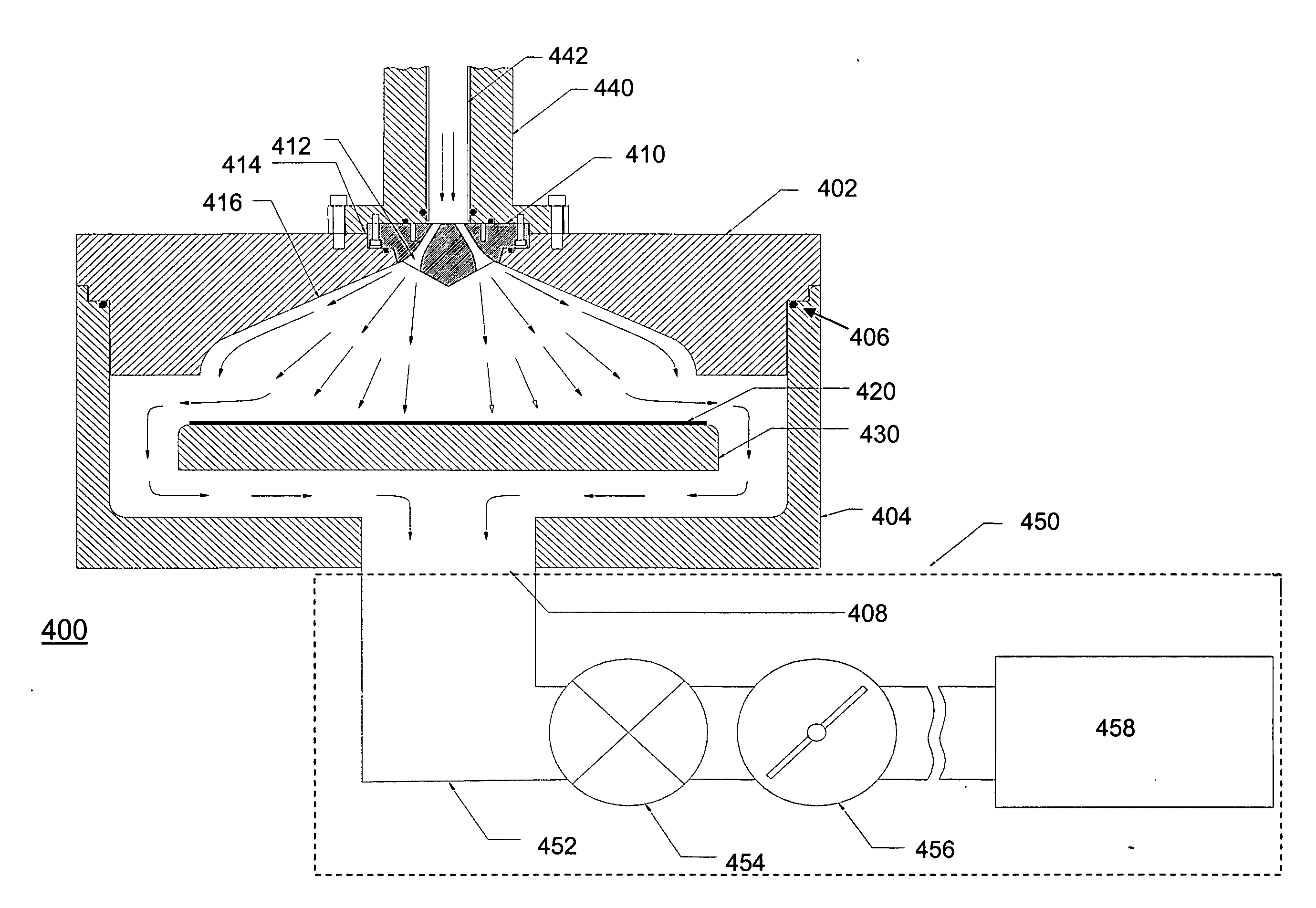
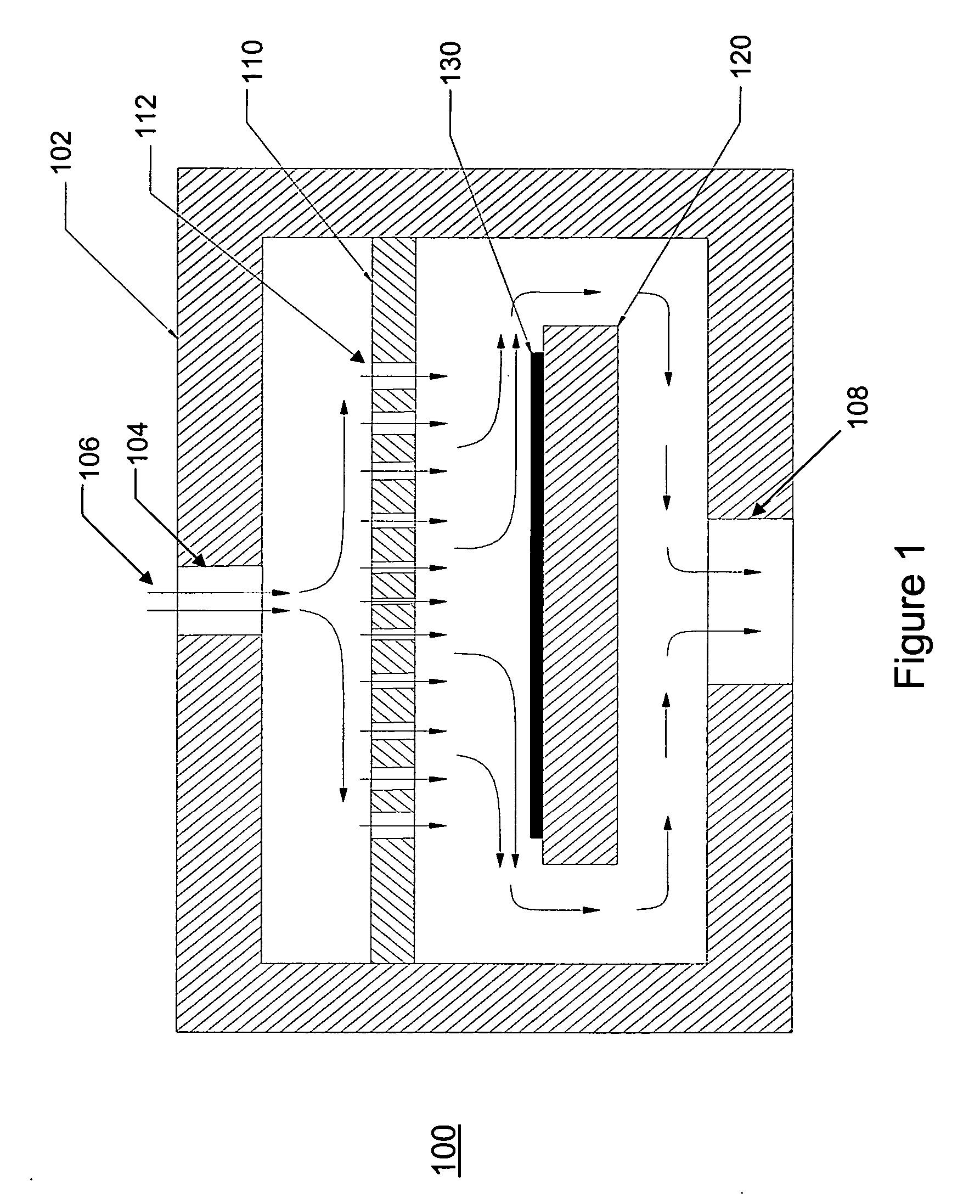
[0029] A gas chamber is described for improving flow of a gas and increasing a strip rate of photoresist on a wafer disposed within the chamber. The gas chamber has a tailored upper chamber body and a gas injector that disperses the gas around the chamber while having a very small surface area to which the gas is exposed. In addition, the gas injector is smaller than known baffles or showerheads, as well as being more economical to manufacture due to its smaller size and relatively simple and short machining process. The term gas, as used herein, includes a gas containing radicals, i.e. a plasma.
[0030] In a stripping process using a gas, typically the gas has a high flow rate and high pressure. As one example, the flow rate of the gas can be 5 standard liters per minute (slm) at 1 Torr. For a gas, the mean free path at this pressure can be obtained with the following equation: L=kT2π Pd2
[0031] where L is the mean free path of the gas, k is the Boltzmann constant, T is the absol...
PUM
| Property | Measurement | Unit |
|---|---|---|
| inclination angle | aaaaa | aaaaa |
| inclination angle | aaaaa | aaaaa |
| pressures | aaaaa | aaaaa |
Abstract
Description
Claims
Application Information