
Field-effect transistor in semiconductor device, method of manufacturing the same

a field-effect transistor and semiconductor device technology, applied in the field of field-effect transistors, can solve problems such as soft errors, and achieve the effect of reducing the area of the semiconductor device and improving the resistance to soft errors

Inactive Publication Date: 2006-10-05
RENESAS ELECTRONICS CORP
View PDF8 Cites 16 Cited by
  • Summary
  • Abstract
  • Description
  • Claims
  • Application Information

AI Technical Summary

Benefits of technology

The present invention provides a field-effect transistor with a cavity design that reduces the occurrence of soft errors and improves the resistance to soft error. By eliminating the substrate around the channel region, the source of electron-hole pairs is isolated, suppressing the soft error. The channel region is formed perpendicular to the substrate surface, while the carriers move parallel to the substrate surface. The method of manufacturing the field-effect transistor includes forming a device isolation region, a trench, a gate insulating film, a gate electrode, diffusion layers, and two cavities. The semiconductor device using the field-effect transistor has improved resistance to soft error and reduced area.

Problems solved by technology

The electron-hole pairs are generated by the incident radiation into the substrate, which causes the soft error.

Method used


Image

  • Field-effect transistor in semiconductor device, method of manufacturing the same
  • Field-effect transistor in semiconductor device, method of manufacturing the same
  • Field-effect transistor in semiconductor device, method of manufacturing the same

Examples


first embodiment

[0047] (Structure)

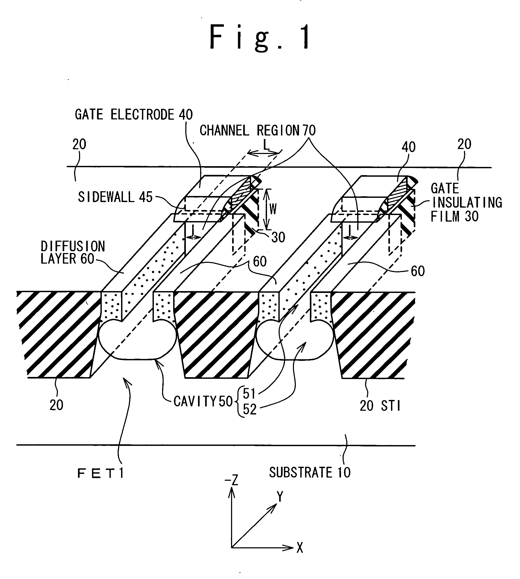
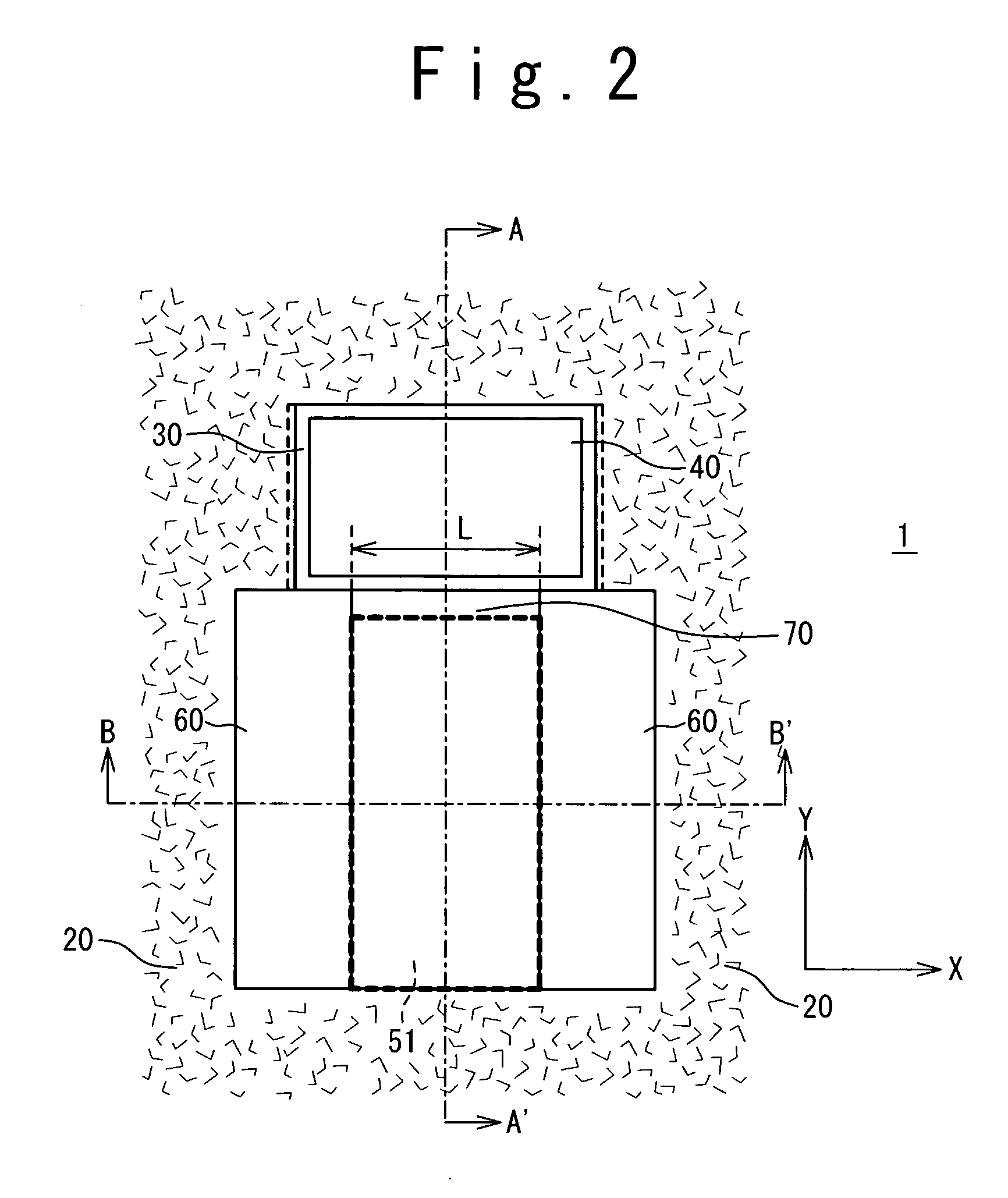
[0048]FIG. 1 is an overall view showing a structure of a field-effect transistor according to a first embodiment. In FIG. 1, a Z-direction (a depth direction) is defined as a direction perpendicular to a surface of a substrate 10. An X-direction and a Y-direction are defined as two directions which are perpendicular to the Z-direction and are orthogonal to each other. That is, a plane parallel to the surface of the substrate 10 is expressed as an XY-plane.

[0049] In FIG. 1, the substrate 10 is provided with an STI 20 which is a device isolation structure (device isolation region) for isolating a device region from another. A field-effect transistor 1 is formed in the device region surrounded by the STIs 20. The field-effect transistor 1 has a gate insulating film 30, a gate electrode 40, and a diffusion layer (source and drain) 60.

[0050] In the present embodiment, the gate insulating film 30 and at least a part of the gate electrode 40 are buried in the substrate...

second embodiment

[0084]FIG. 5A is a cross sectional view showing a structure of a field-effect transistor according to a second embodiment of the present invention. FIG. 5A is a figure corresponding to FIG. 3B mentioned above, and shows a structure in the XZ-plane. In FIG. 5A, the same reference numeral as that in FIG. 3B is given to the same structure as that in FIG. 3B, and description thereof is appropriately omitted. FIG. 5B is a cross sectional view showing a part of processes of manufacturing the field-effect transistor according to the present embodiment. FIG. 5B is a figure corresponding to FIG. 4I mentioned above. In FIG. 5B, the same reference numeral as that in FIG. 4I is given to the same structure as that in FIG. 4I, and description thereof is appropriately omitted.

[0085] According to the present embodiment, a protection film 55 is not formed on the side wall of the first cavity 51. Not only a bottom surface but also a side surface of the diffusion layer 60 is exposed to the cavity 50....

third embodiment

[0086]FIG. 6A is a cross sectional view showing a structure of a field-effect transistor according to a third embodiment of the present invention. FIG. 6A is a figure corresponding to FIG. 3B mentioned above, and shows a structure in the XZ-plane. In FIG. 6A, the same reference numeral as that in FIG. 3B is given to the same structure as that in FIG. 3B, and description thereof is appropriately omitted. FIG. 6B is a cross sectional view showing a part of processes of manufacturing the field-effect transistor according to the present embodiment. FIG. 6B is a figure corresponding to FIG. 4I mentioned above. In FIG. 6B, the same reference numeral as that in FIG. 4I is given to the same structure as that in FIG. 4I, and description thereof is appropriately omitted.

[0087] According to the present embodiment, a bottom surface of the diffusion layer 60 does not reach a second cavity 52. In other words, the diffusion layer 60 is formed in only a part of a region surrounded by the cavity 50...


PUM


Abstract

A field-effect transistor has: a substrate having a first cavity; a gate electrode buried in the substrate; and diffusion layers formed in the substrate and being in contact with the first cavity. A channel region is formed substantially perpendicular to a surface of the substrate between the diffusion layers.

Description

BACKGROUND OF THE INVENTION [0001] 1. Field of the Invention [0002] The present invention relates to a transistor technology. In particular, the present invention relates to a field-effect transistor, a method of manufacturing the same, a semiconductor device and a semiconductor memory device having the field-effect transistor. [0003] 2. Description of the Related Art [0004] Incident radiation (cosmic ray, thermal neutron, α-ray and so on) into a semiconductor memory device generates electron-hole pairs due to collision with a silicon substrate. The generated electron-hole pairs are collected in a diffusion layer, which causes a change in potential at a node. What most contributes to the potential change at the node is funneling immediately under a drain region among charge collection mechanisms. A phenomenon that a memory cell data is rewritten due to the potential change at the node is called a “soft error”. With the advance of miniaturization of a device in recent years, the infl...

Claims


Application Information

Patent Timeline
Patent Type & Authority Applications(United States)
IPC IPC(8): H01L29/94
CPCH01L21/28273H01L27/10873H01L27/10876H01L27/11H01L27/1104H01L29/7881H01L27/11517H01L29/42336H01L29/66621H01L29/66825H01L27/115H01L29/40114H10B12/05H10B12/053H10B10/00H10B10/12H10B41/00H10B69/00
Inventor HASHIMOTO, SHINGO
Owner RENESAS ELECTRONICS CORP
Learn More