Conductive bump structure of circuit board and fabrication method thereof

a technology of conductive bumps and circuit boards, which is applied in the direction of printed circuits, conductive pattern formation, non-metallic protective coating applications, etc., can solve the problems of increasing the number of electrically connecting pads, increasing the requirement of registration, and increasing the area of chip carriers, so as to reduce the requirement of registration and increase the contact area between the conductive bump structure and the terminals. , the effect of increasing the contact area

Inactive Publication Date: 2006-10-12
PHOENIX PRECISION TECH CORP
View PDF5 Cites 24 Cited by
  • Summary
  • Abstract
  • Description
  • Claims
  • Application Information

AI Technical Summary

Benefits of technology

[0028] Compared with the prior art that forms conductive bumps on electrically connecting pads, the present invention forms fine pitch conductive bumps on terminals of conductive circuits, thereby avoiding the prior art drawbacks such as fabrication difficulty due to high requirement of registration and difficulty of forming fine pitch conductive bumps when the registration resolution is reduced. In addition, because the conductive bumps of the present invention completely co

Problems solved by technology

However, with reduced size and increased input/output terminals of semiconductor chips, the area of chip carriers is becoming smaller and the number of electrically connecting pads is increasing.
With reduced size of electrically connecting pads, size of the stencil openings need to be reduced correspondingly, which not only results in high fabrication cost, but also makes the solder material difficult to pass through.
Furthermore, as the solder material is viscose, the more frequent performances of stencil printing leave more the solder material remaining on the inner walls of the stencil openings, which would make the amount and shape of the solder material in subsequent printing processes not match the predetermined design.
As a result, the size of the electrically connecting pads 301 (D3) is not easy to be reduced, which accordingly cannot meet the requirement of fine pitch circuit.
In the above electroplating process, to ach

Method used


Image

  • Conductive bump structure of circuit board and fabrication method thereof
  • Conductive bump structure of circuit board and fabrication method thereof
  • Conductive bump structure of circuit board and fabrication method thereof

Examples


Embodiment Construction

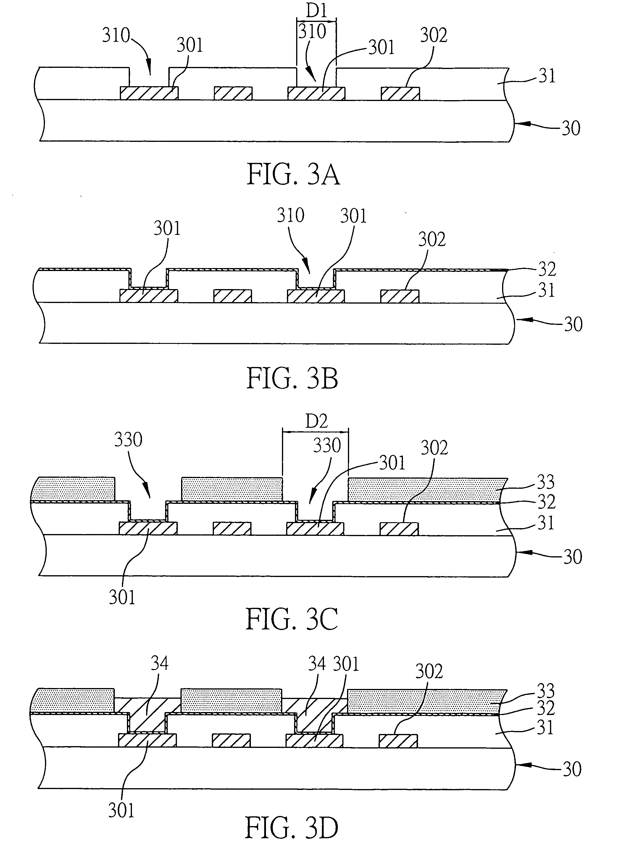
[0035] Embodiments of a conductive bump structure of a circuit board and a fabrication method thereof proposed in the present invention are described with reference to FIGS. 4A to 4I and 4I′.

[0036]FIGS. 4A to 4I show a fabrication method of a conductive bump structure of a circuit board according to the present invention. It should be noted that the drawings only show basic construction related to the present invention.

[0037] Referring to FIG. 4A, an insulating layer 41 is formed on a core circuit board 40 with electrically connecting pads 401 and conductive circuits 402 formed on one surface thereof, the insulating layer 41 having a plurality of openings 410 to expose the electrically connecting pads 401.

[0038] Referring to FIG. 4B, a conductive layer 42 is formed on the insulating layer 41 and surface of the openings 410 to function as a current conductive path in subsequent electroplating process. The conductive layer 42 can be a metal layer or several laminated metal layers f...


PUM

PropertyMeasurementUnit
Sizeaaaaaaaaaa
Electrical conductoraaaaaaaaaa
Widthaaaaaaaaaa

Abstract

A conductive bump structure of a circuit board and a fabrication method thereof are proposed. The circuit board is formed with conductive circuits on a surface thereof An insulating protection layer having a plurality of openings to expose terminals of the conductive circuits is formed on the circuit board. A conductive layer is formed on the insulating protection layer and in the openings thereof. A patterned resist layer is formed on the conductive layer and has a plurality of openings corresponding in position to the terminals of the conductive circuits. Conductive bumps are formed by electroplating in the openings of the resist layer. Then, the resist layer and the conductive layer underneath the resist layer are removed. An adhesive layer is formed on the conductive bumps and completely covers exposed surfaces of the conductive bumps respectively. The circuit board can be electrically connected to electronic elements through the conductive bumps.

Description

FIELD OF THE INVENTION [0001] The present invention relates to fabrication methods of conductive bump structures of circuit boards, and more particularly, to a conductive bump structure of a circuit board for electrical connection with an external device, and a fabrication method of the conductive bump structure by electroplating. BACKGROUND OF THE INVENTION [0002] Compared with the wire bond technique, the flip-chip package proposed by IBM Inc. in 1960 uses solder bumps instead of golden wires to electrically connect a semiconductor chip with a substrate, thereby increasing package density, reducing package size and enhancing electrical performance. According to these advantages, a control-collapse chip connection (C4) is proposed which applies high temperature solder on a ceramic substrate. [0003] According to the current flip-chip technique, a semiconductor IC chip surface is provided with electrode pads and correspondingly, a circuit board is provided with electrically connectin...

Claims


Application Information

Patent Timeline
IPC IPC(8): H05K1/09H05K3/12
CPCH05K1/113H05K3/28H05K3/4007H05K3/423Y10T29/49147H05K2201/09563H05K2201/096H05K2203/054H05K2201/09436
Inventor HU, WEN-HUNG
Owner PHOENIX PRECISION TECH CORP
Why Eureka
Try Eureka