

Gas barrier film, substrate film, and organis electroluminescence device
a technology of gas barrier film and substrate, which is applied in the field of gas barrier film, can solve the problems of poor gas barrier property of film substrate, difficult to increase the area, and difficult to increase the area, and achieve the effects of high viscosity, difficult film formation, and sometimes deteriorating dynamic characteristics
- Summary
- Abstract
- Description
- Claims
- Application Information
AI Technical Summary
Benefits of technology
Problems solved by technology
Method used
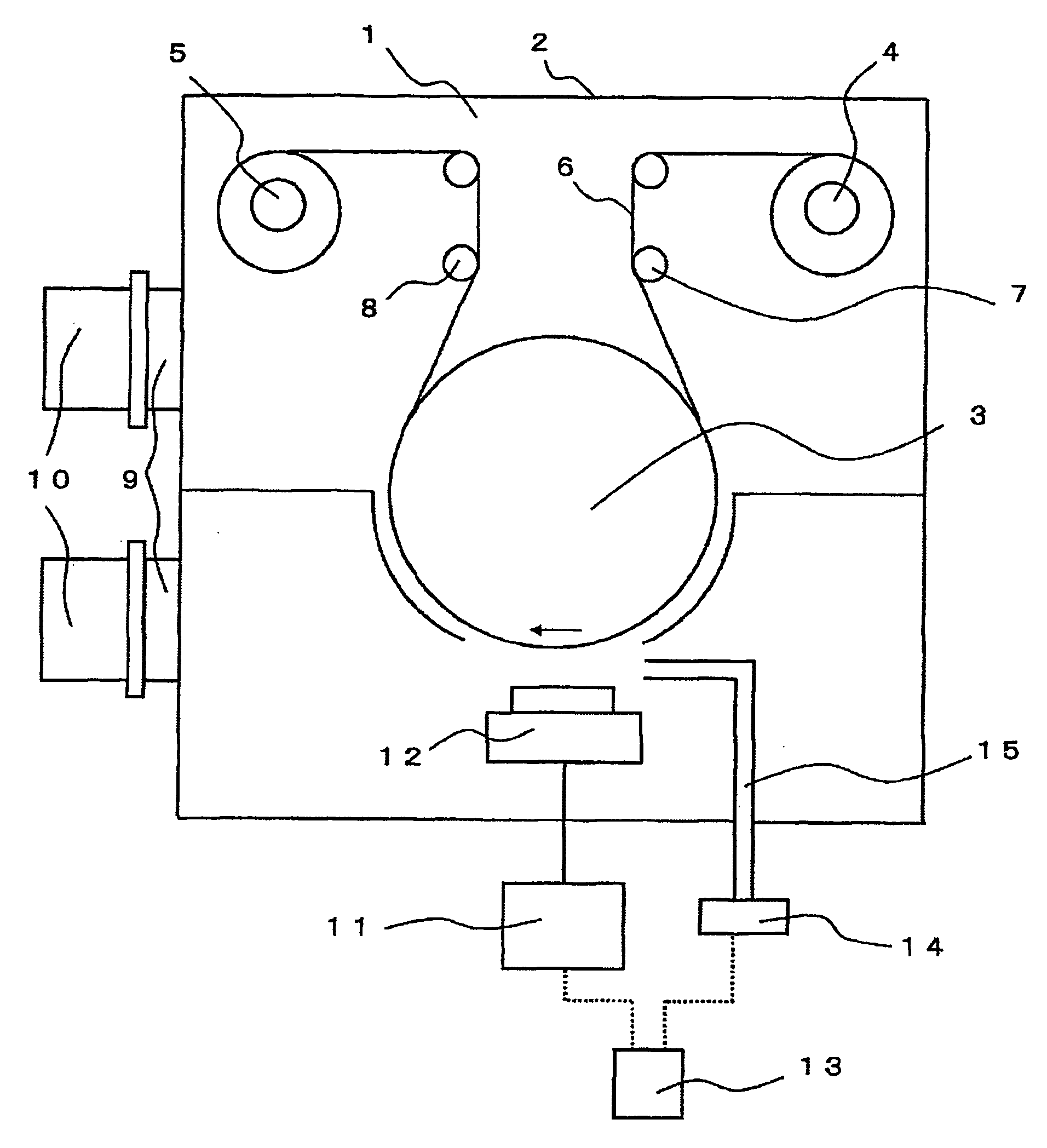
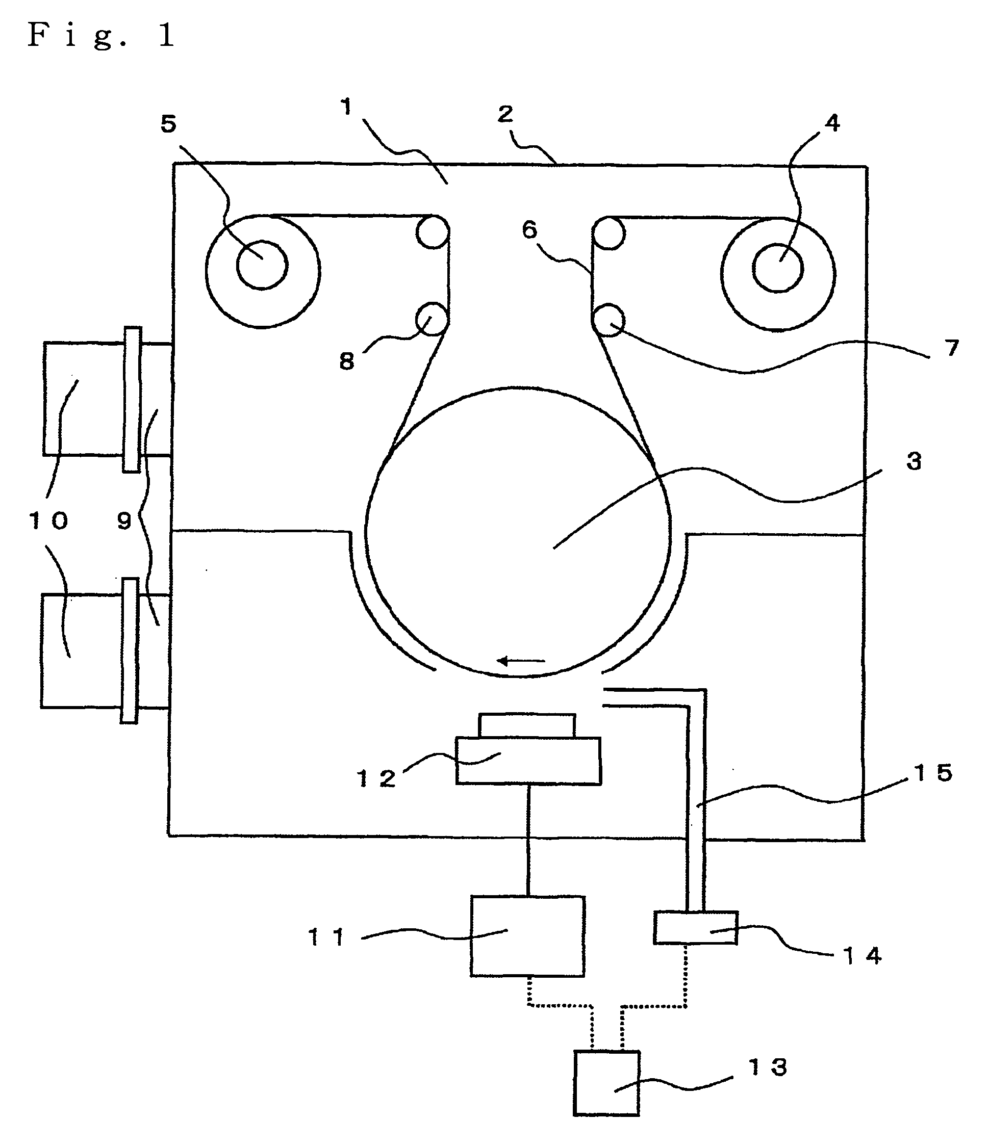
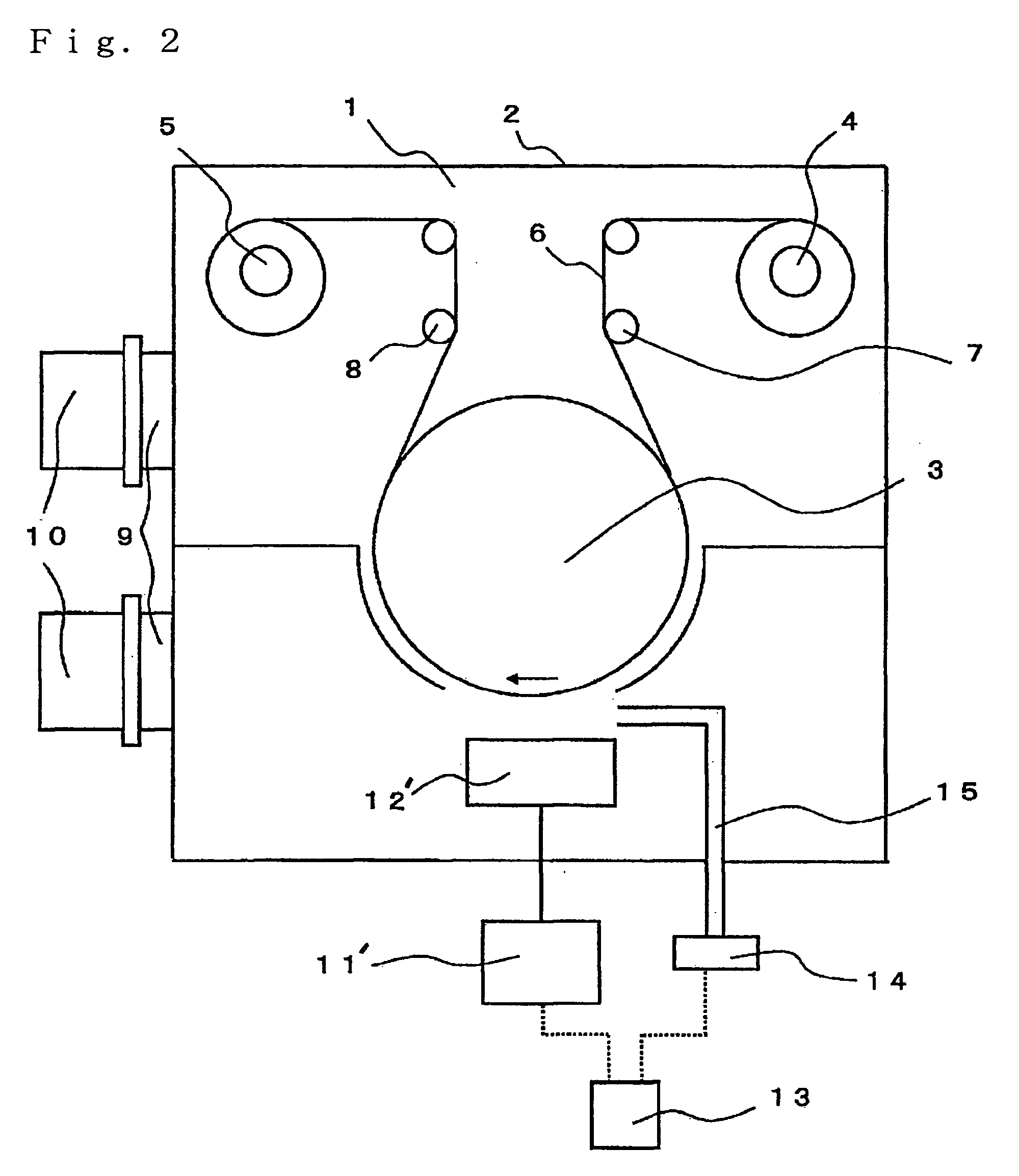
Image

Examples
example 1
[0143] Gas barrier films each formed by disposing a gas barrier laminate on a substrate film and a transparent conductive layer thereon (Sample Nos. 1 to 21) were prepared in accordance with the following procedures. Details for the structure of each of the gas barrier films are as described in Table 1 and Table 2.
(1) Preparation of Substrate Film
[0144] Substrate films of 100 μm thickness comprising resins described in Table 1 were provided. In Table 1, Lumilar T60 manufactured by Toray Co. was used as PET, and Teonex Q65AF manufactured by Teijin Dupont Film Co. was used as PEN. Further, the substrate films used for Samples Nos. 8 to 14 were prepared from the resins as the starting materials by the following method.
[0145] The resin was dissolved in a dichloromethane solution such that the concentration was 15 mass % and the solution was cast by a die coating method over a stainless steel band. Then, the first film was peeled from the band and dried till the residual solvent conc...
example 2
[0165] An anode of an indium tin oxide (ITO, indium / tin=95 / 5 molar ratio) was formed on a gas barrier film of 25 mm×25 mm (Samples Nos. 1 to 21) using a DC power source by a sputtering method (0.2 μm thickness). Copper phthalocyanine (CuPc) was formed as a hole injecting layer to 10 nm on the anode by a vacuum vapor deposition method, on which N,N′-dinaphthyl-N,N′-diphenyl benzidine was formed as the hole transporting layer to 40 nm by a vacuum vapor deposition method. 4,4′-N,N′-diarbazole biphenyl was formed thereon as the host material, bis[(4,6-difluorophenyl)-pyridinate-N, C2′] (picolinate) iridium complex (Firpic) as the blue color emitting material, tris(2-phenylpyridine) iridium complex (Ir(ppy)3) as the green color emitting material and bis(2-phenylquinoline) acetyl acetonate iridium as the red light emitting material were co-vapor deposited to at a weight ratio of 100 / 2 / 4 / 2 respectively, to obtain a light emitting layer of 40 nm. Further, 2,2′,2″-(1,3,5-benzene toluyl)tris[...
PUM
| Property | Measurement | Unit |
|---|---|---|
| glass transition temperature | aaaaa | aaaaa |
| refractive index | aaaaa | aaaaa |
| refractive index | aaaaa | aaaaa |
Abstract
Description
Claims
Application Information