Semiconductor device and method of manufacturing semiconductor device

a semiconductor and semiconductor technology, applied in semiconductor devices, solid-state devices, basic electric elements, etc., can solve the problems of high cost, increase of manufacturing costs of the entire semiconductor device, and large size of the silicon interposer substrate, so as to reduce the plane and reduce the size of the semiconductor substra

Active Publication Date: 2006-10-12
SONY CORP
View PDF1 Cites 184 Cited by
  • Summary
  • Abstract
  • Description
  • Claims
  • Application Information

AI Technical Summary

Benefits of technology

[0021] There is no need to form on the semiconductor substrate, pads having comparatively large size and pitch that meet the design rule of the wiring board for connection to the wiring board. That is, it is sufficient for the semiconductor substrate to have thereon, as pads, only the chip-connection pads having finer size and pitch for connection to the semiconductor chips. Therefore, the plane size of the semiconductor substrate can be decreased, which allows the reduction of costs of the semiconductor substrate.
[0022] The semiconductor chips are connected to the external (wiring board) via the external-connection pads provided directly on the semiconductor chips, without the intermediary of the semiconductor substrate. Therefore, compared with the above-described Patent Document 2, in which semiconductor chips are connected to a wiring board via a semiconductor substrate, the length of interconnections between the semiconductor chips and wiring board can be decreased, which can suppress delay of signal transmission between the semiconductor chips and wiring board.
[0023] Moreover, as to interconnections, the semiconductor substrate has thereon only the chip-to-chip interconnection but does not have interconnections for connecting the semiconductor chips to the wiring board. Therefore, the chip-to-chip interconn

Problems solved by technology

Silicon etching for forming the through vias and the precipitation of the conductive portions 56 by plating in the through vias take high costs and long time periods, which problematically results in an increase of manufacturing costs of the entire semiconductor device.
Due to this large pitch of the pads 49, the size of the silicon interposer substrate 53 in the plane d

Method used


Image

  • Semiconductor device and method of manufacturing semiconductor device
  • Semiconductor device and method of manufacturing semiconductor device
  • Semiconductor device and method of manufacturing semiconductor device

Examples


first embodiment

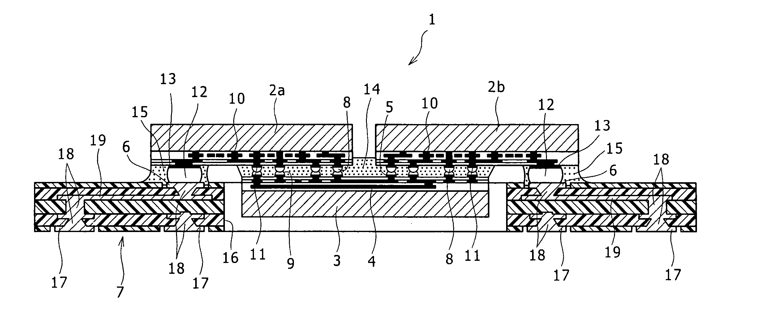
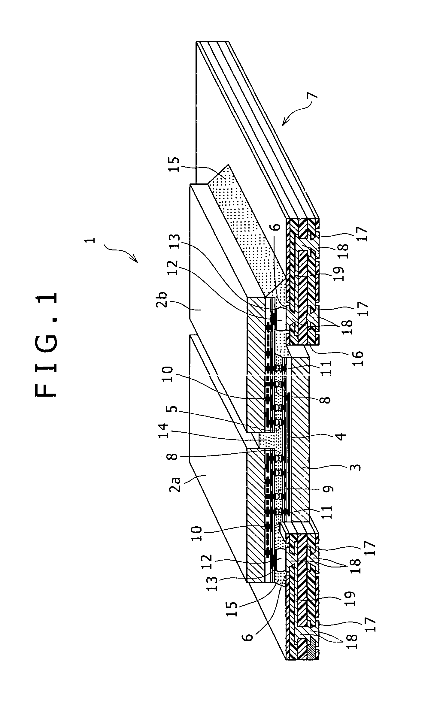
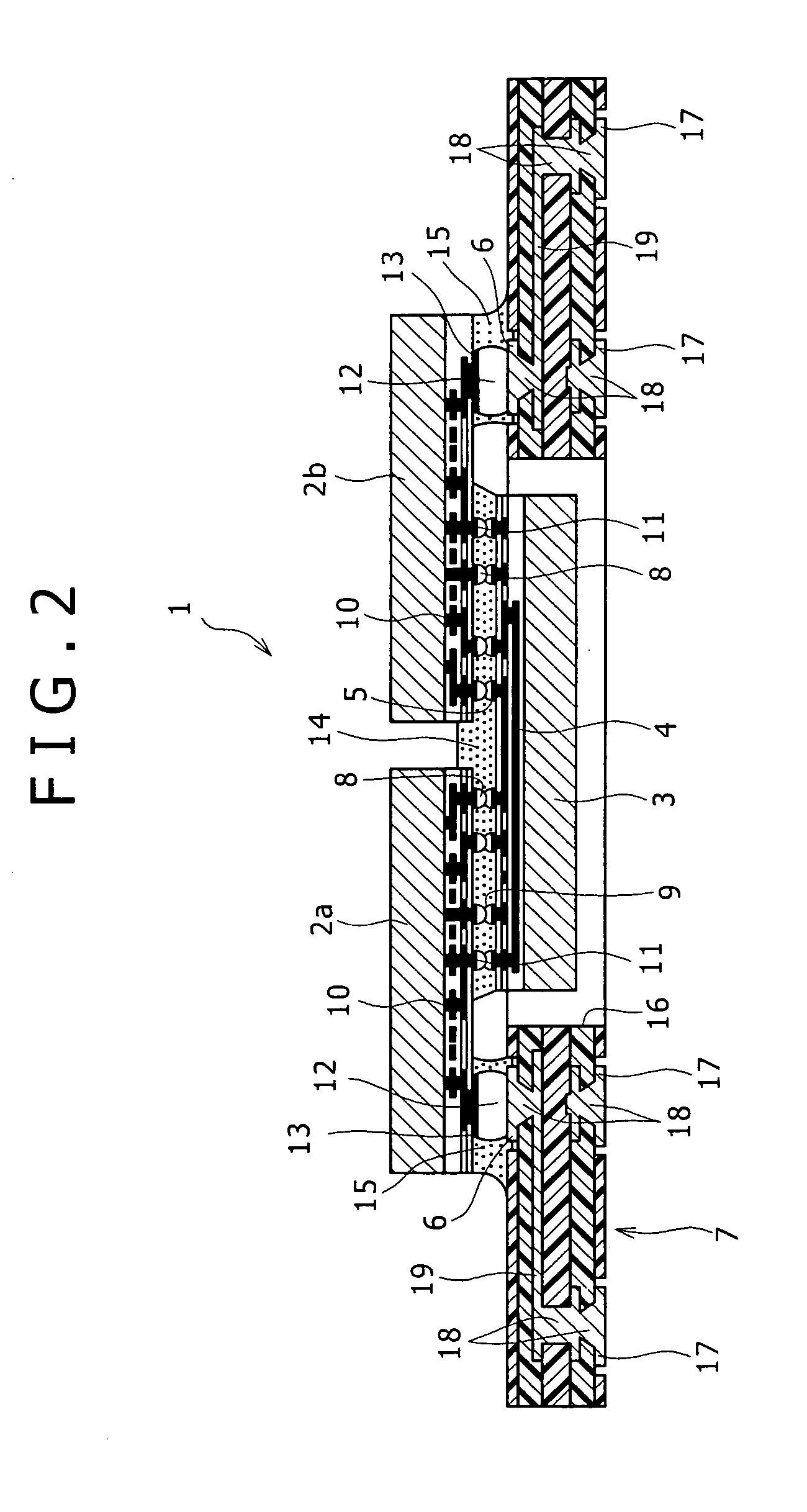
[0045]FIG. 1 is a partially sectional perspective view illustrating a semiconductor device 1 according to a first embodiment of the present invention. FIG. 2 is a sectional view illustrating the semiconductor device 1.

[0046] The semiconductor device 1 includes a semiconductor substrate 3, a plurality of semiconductor chips 2a and 2b mounted on the semiconductor substrate 3, and a wiring board 7 connected to the semiconductor chips 2a and 2b.

[0047] The semiconductor substrate 3 has, on the same surface thereof, chip-to-chip interconnections 4 for electrically connecting the semiconductor chips 2a and 2b to each other, and a plurality of chip-connection pads 5 connected to the chip-to-chip interconnections 4.

[0048] The major surfaces (IC-formed surfaces) of the semiconductor chips 2a and 2b are connected via first connectors 8 and 9 to the chip-connection pads 5 on the semiconductor substrate 3. Thus, the semiconductor chips 2a and 2b are electrically connected to each other via th...

second embodiment

[0075]FIG. 9 is a partially sectional perspective view illustrating a semiconductor device 21 according to a second embodiment of the present invention. FIG. 10 is a sectional view illustrating the semiconductor device 21. The same parts as those in the first embodiment are given the same numerals, and detailed description thereof will be omitted.

[0076] The semiconductor device 21 of the present embodiment includes a semiconductor substrate 3, a plurality of semiconductor chips 2a and 2b mounted on the semiconductor substrate 3, and a wiring board 27 connected to the semiconductor chips 2a and 2b.

[0077] The semiconductor substrate 3 has, on the same surface thereof, chip-to-chip interconnections 4 for electrically connecting the semiconductor chips 2a and 2b to each other, and a plurality of chip-connection pads 5 connected to the chip-to-chip interconnections 4.

[0078] The major surfaces (IC-formed surfaces) of the semiconductor chips 2a and 2b are connected via first connectors ...

third embodiment

[0091]FIG. 13 illustrates a semiconductor device 31 according to a third embodiment of the present invention. The same parts as those in the first and second embodiments are given the same numerals, and detailed description thereof will be omitted.

[0092] The semiconductor device 31 of the present embodiment includes a semiconductor substrate 3, a plurality of semiconductor chips 2a and 2b mounted on the semiconductor substrate 3, and a wiring board 37 connected to the semiconductor chips 2a and 2b.

[0093] The semiconductor substrate 3 has, on the same surface thereof, chip-to-chip interconnections 4 for electrically connecting the semiconductor chips 2a and 2b to each other, and a plurality of chip-connection pads 5 connected to the chip-to-chip interconnections 4.

[0094] The major surfaces (IC-formed surfaces) of the semiconductor chips 2a and 2b are connected via first connectors 8 and 9 to the chip-connection pads 5 on the semiconductor substrate 3. Thus, the semiconductor chips...


PUM


Abstract

The present invention provides a semiconductor device that is inexpensive and can suppress signal transmission delay, and a manufacturing method thereof. The semiconductor device includes: a plurality of semiconductor chips; a semiconductor substrate that has, on the same surface thereof, a chip-to-chip interconnection for electrically connecting the plurality of semiconductor chips to each other, and a plurality of chip-connection pads connected to the chip-to-chip interconnection; and a wiring board that has a plurality of lands of which pitch is larger than a pitch of the chip-connection pads, wherein a major surface of each of the plurality of semiconductor chips is connected to the chip-connection pads via a first connector so that the plurality of semiconductor chips are mounted on the semiconductor substrate, and an external-connection pad is formed on the major surface other than a region facing the semiconductor substrate, and is connected to the land on the wiring board via a second connector.

Description

CROSS REFERENCES TO RELATED APPLICATIONS [0001] The present invention contains subject matter related to Japanese Patent Application JP 2005-075165 filed in the Japanese Patent Office on Mar. 16, 2005, the entire contents of which being incorporated herein by reference. BACKGROUND OF THE INVENTION [0002] The present invention relates to semiconductor devices referred to as a so-called system in package, in which a plurality of semiconductor chips are mounted in one package form, and manufacturing methods thereof. The invention relates more particularly to a semiconductor device having a structure in which a semiconductor substrate is used to electrically coupling a plurality of semiconductor chips, and a manufacturing method thereof. [0003] Recent trends of electronic apparatuses toward higher functions are requiring that semiconductor chips used in the apparatuses also have higher functions. However, an attempt to achieve higher functions with a system on chip (SoC) approach, in wh...

Claims


Application Information

Patent Timeline
IPC IPC(8): H01L23/02H01L21/00
CPCH01L23/5389H01L2924/10253H01L2924/15311H01L2224/16145H01L2224/16225H01L2224/32145H01L2224/32225H01L2224/73204H01L2924/15153H01L2924/15192H01L2924/157H01L25/0655H01L2224/1703H01L2924/00H01L2224/05022H01L2224/05026H01L2224/05568H01L2224/05023H01L2224/05001H01L2224/051H01L2224/05624H01L2224/05647H01L2224/0603H01L2224/02379H01L24/05H01L2224/1403H01L2924/15151H01L2924/00014E04C2/292E04B1/6125
Inventor HATANO, MASAKITAKAOKA, YUJI
Owner SONY CORP
Why Eureka
Try Eureka