Semiconductor memory device and method for manufacturing semiconductor device

a memory device and semiconductor technology, applied in the direction of semiconductor devices, electrical appliances, transistors, etc., can solve the problems of deterioration of the film quality of the lower silicon oxide film, the increase of the demand for miniaturization and high performance of the semiconductor memory, and the multi-layered insulating film. achieve the effect of high reliability and high quality

a memory device and semiconductor technology, applied in the direction of semiconductor devices, electrical appliances, transistors, etc., can solve the problems of deterioration of the film quality of the lower silicon oxide film, the increase of the demand for miniaturization and high performance of the semiconductor memory, and the multi-layered insulating film. achieve the effect of high reliability and high quality

US20060228899A1Inactive Publication Date: 2006-10-12SPANSION LLC

Image

  • Semiconductor memory device and method for manufacturing semiconductor device
  • Semiconductor memory device and method for manufacturing semiconductor device
  • Semiconductor memory device and method for manufacturing semiconductor device

Examples


specific embodiments

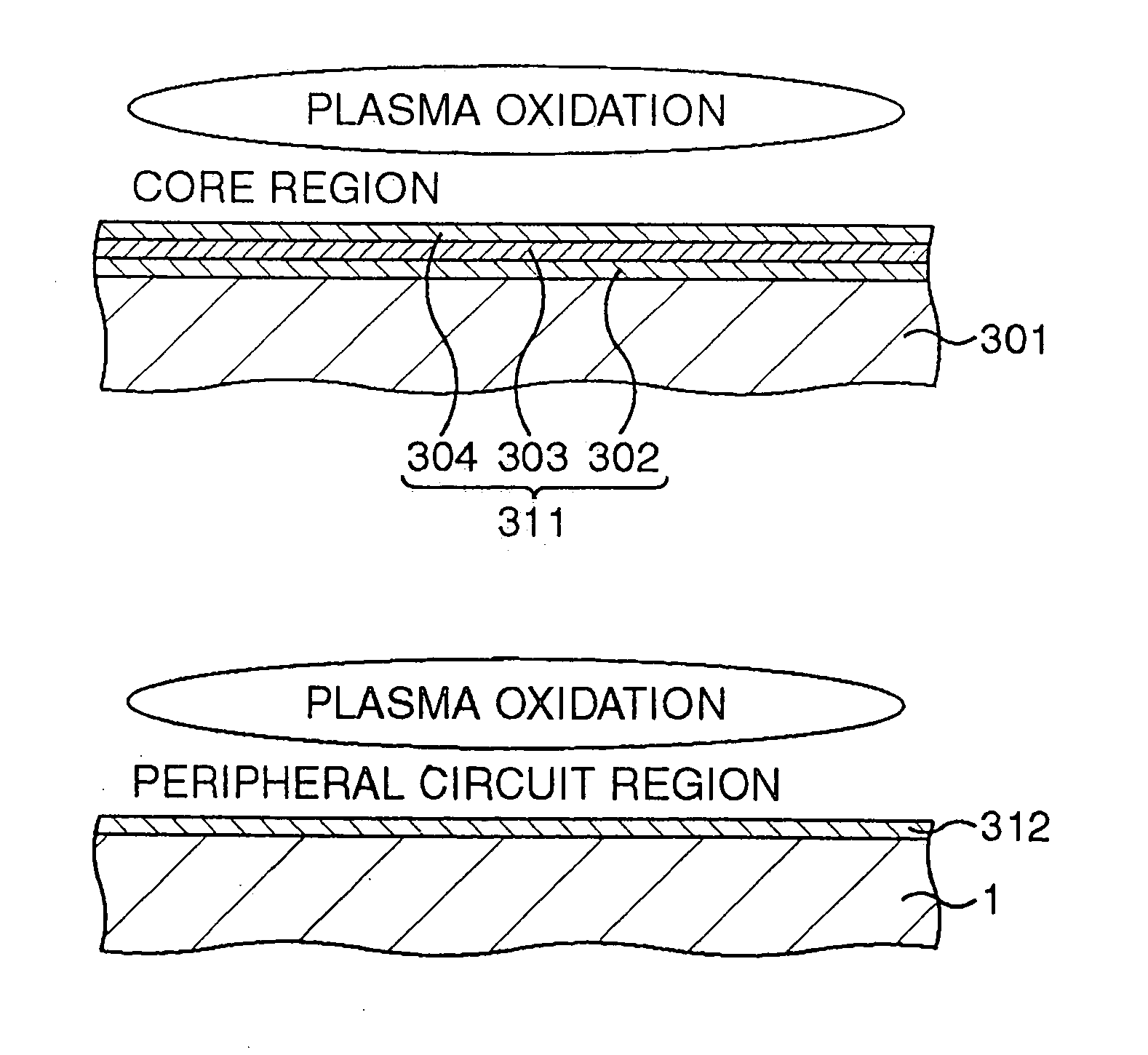
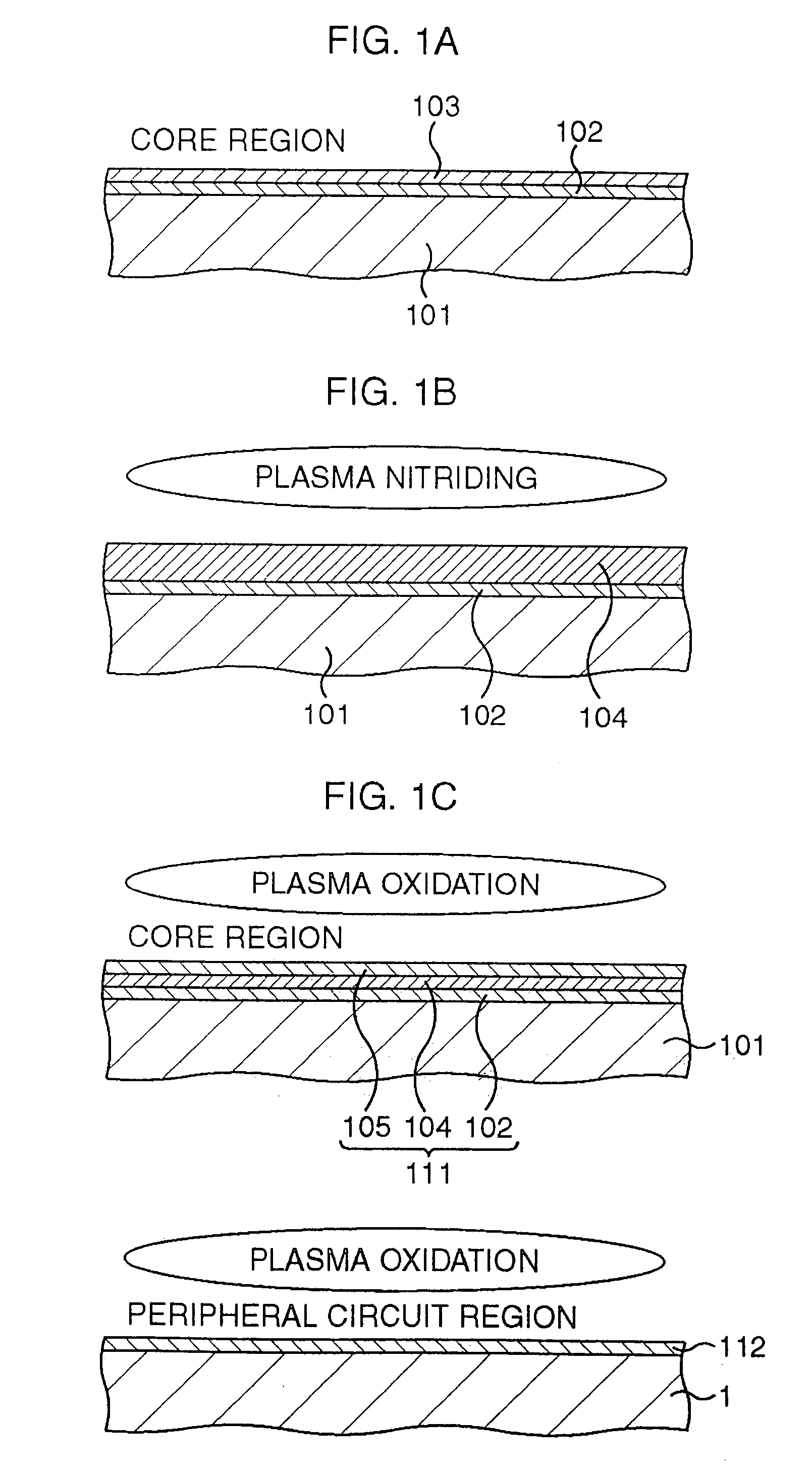
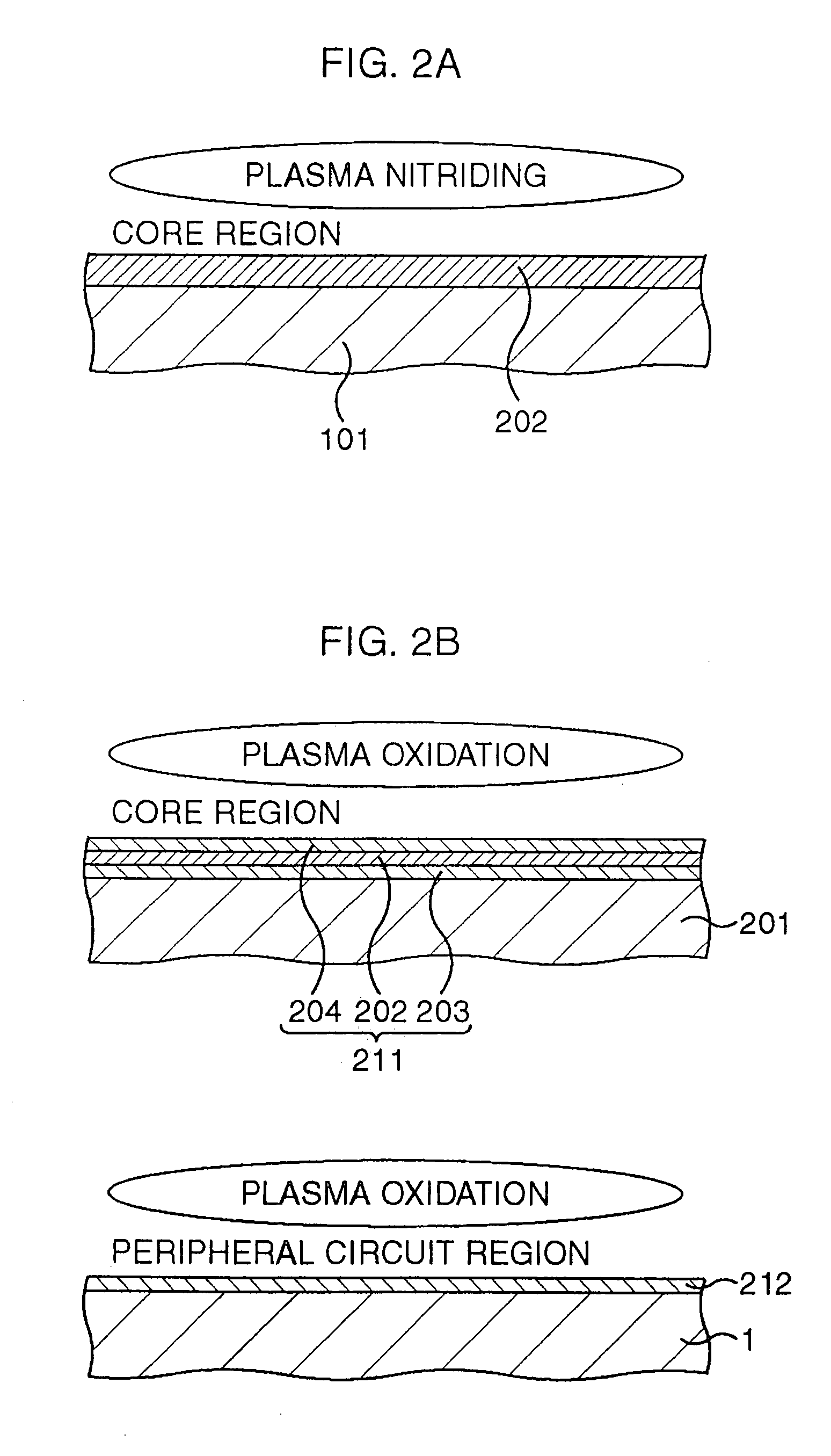
[0086] Specific embodiments are explained below based on the aforementioned basic structure of the present invention.

first embodiment

[0087] In this embodiment, a semiconductor memory device having an embedded bit line type SONOS structure will be disclosed. A structure of the semiconductor memory device is explained with a method for manufacturing thereof as a matter of convenience.

[0088] This semiconductor memory device is so structured that SONOS transistors in a memory cell region are of a planer type and that CMOS transistors are formed in a peripheral circuit region.

[0089]FIG. 4A to FIG. 13B are schematic cross sectional views showing a method for manufacturing the semiconductor memory device including embedded bit line type SONOS transistors in this embodiment in the order of processes. Here, each A of the drawings shows a memory cell region (a core region), and each B thereof shows a peripheral circuit region. The left side of the A thereof corresponds to a cross section (an X section) taken along the parallel line to a gate electrode (a word line), and the right side corresponds to a cross section (a Y ...

second embodiment

[0122] In this embodiment, a floating gate type semiconductor memory device will be disclosed. A structure of the semiconductor memory device is explained with a method for manufacturing thereof as a matter of convenience.

[0123] The floating gate type transistors are formed in a memory cell region, and CMOS transistors are formed in a peripheral circuit region.

[0124]FIG. 15A to FIG. 26B are schematic cross sectional views showing a method for manufacturing the semiconductor memory device including the floating gate type transistors in this embodiment in the order of processes. It should be noted that, for convenience, the same reference numerals are given to the components or the like explained in the first embodiment. Here, each A of the drawings except FIG. 20 shows a memory cell region (a core region), and each B thereof shows a peripheral circuit region. The left side of the A thereof corresponds to a cross section (an X section) taken along the parallel line to a control gate...


PUM

PropertyMeasurementUnit
thicknessaaaaaaaaaa
temperatureaaaaaaaaaa

Abstract

After a lower silicon oxide film is formed on a silicon region, a silicon film is formed on the lower silicon oxide film by, for example, a thermal CVD method. Subsequently, the silicon film is completely nitrided by a plasma nitriding method to be replaced by a silicon nitride film. Subsequently, a surface layer of the silicon nitride film is oxidized by a plasma oxidizing method to be replaced by an upper silicon oxide film. An ONO film as a multilayered insulating film composed of the lower silicon oxide film, the silicon nitride film, and the upper silicon oxide film is formed.

Description

CROSS-REFERENCE TO RELATED APPLICATIONS [0001] This application is a division of application Ser. No. 10 / 643,967 filed Aug. 20, 2003, based upon and claims the benefit of priority from the prior Japanese Patent Application No. 2002-256195, filed on Aug. 30, 2002, the entire contents of which are incorporated herein by reference. BACKGROUND OF THE INVENTION [0002] 1. Field of the Invention [0003] The present invention relates to a method for manufacturing a semiconductor device having a gate insulation film or a dielectric film including a nitrided film, and a semiconductor memory device capable of holding information by storing electric charges in the nitrided film. [0004] 2. Description of the Related Art [0005] Recently, an ON film composed of a silicon nitride film formed on a silicon oxide film, and an ONO film composed of a silicon oxide film, a silicon nitride film, and a silicon oxide film formed in this order are used for a memory cell of a semiconductor memory device. [0006...

Claims


Application Information

Patent Timeline
12 Oct 2006
Publication
US20060228899A1
IPC
H01L21/31; H01L21/336; H01L21/318; H01L21/8247; H01L27/10; H01L29/788; H01L29/792; H10B20/00; H10B69/00; H10B99/00
CPC
H01L21/3145; H01L27/105; Y10S438/954; H01L27/11546; H01L27/11568; H01L27/11526; H01L21/02164; H01L21/022
Inventors
NANSEI, HIROYUKI; NAKAMURA, MANABU