Multilayer printed wiring board

a printing board and wiring board technology, applied in the direction of printed element electric connection formation, dielectric characteristics, semiconductor/solid-state device details, etc., can solve the problems of wiring layer cracks at the external portions of the ic chip, interference with the attainment of higher speeds, signal delays in wiring layers becoming dominant, etc., to achieve the effect of simple preparation

Active Publication Date: 2006-10-19
IBIDEN CO LTD
View PDF7 Cites 44 Cited by
  • Summary
  • Abstract
  • Description
  • Claims
  • Application Information

AI Technical Summary

Benefits of technology

[0013] In the multilayer printed wiring board of the invention, it is preferable that, among the conductor posts, at least the external conductor posts are formed to have a shape with a constriction. The effects of the invention can be obtained more assuringly in comparison to the case where the conductor posts are of substantially straight shape. In the multilayer printed wiring board of the invention, the maximum diameter/minimum diameter of the external conductor posts that are formed to have a shape with a constriction is preferably not less than 2 and not more than 4.
[0014] In the multilayer printed wiring board of the invention, when the conductor posts are formed to have multiple arrays from an outermost array to an N-th array (where N is an integer of 2 or more), it is preferably that the conductor posts within a range from the outermost array to the (N×⅔)-th array are set to the external conductor posts. The stress that is applied to the conductor posts within this range is large in comparison to the stress applied to the other conductor posts. It is thus significant to apply the present invention. When N is 15, for example, the external conductor posts will be determined as conductor posts within the range from the outermost array to the tenth array, and the external conductor posts may be conductor posts in just the single outermost array, or conductor posts from the outermost array to the second array, . . . , or conductor posts from the outermost array to the tenth array.
[0015] In the multilayer printed wiring board of the invention, the low elastic modulus layer maybe formed so as to be substantially matched with the entirety of a virtual projection of the electronic element onto the low elastic modulus layer. The low elastic modulus layer may be formed beyond the entire area of this projected portion, however, since adequate effects will be provided if the low

Problems solved by technology

However, as wirings are made finer, signal delays in wiring layers become dominant and interfere with attaining higher speeds.
However, when heating and cooling are repeated with an IC chip that has porous interlayer insulating films and is mounted on a multilayer printed wiring board, the stress relaxing layer disclos

Method used


Image

  • Multilayer printed wiring board
  • Multilayer printed wiring board
  • Multilayer printed wiring board

Examples


examples

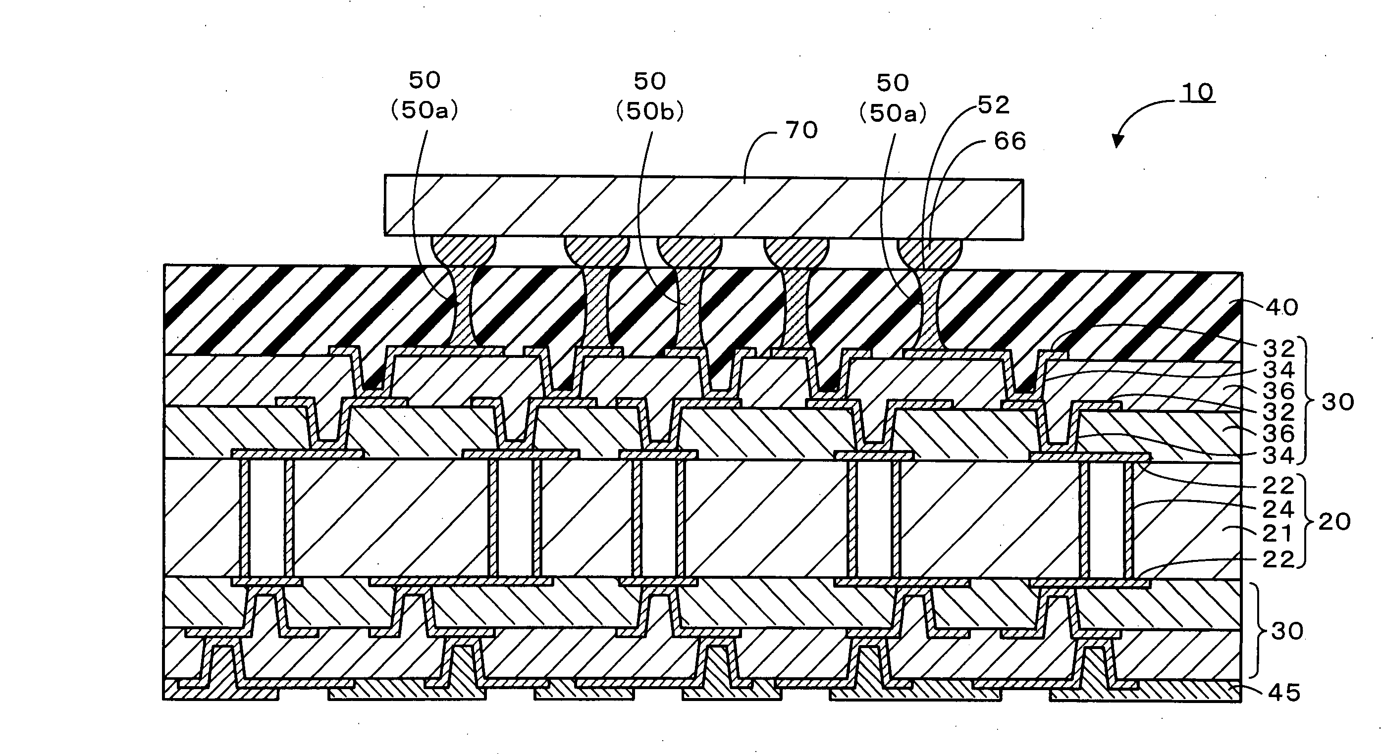
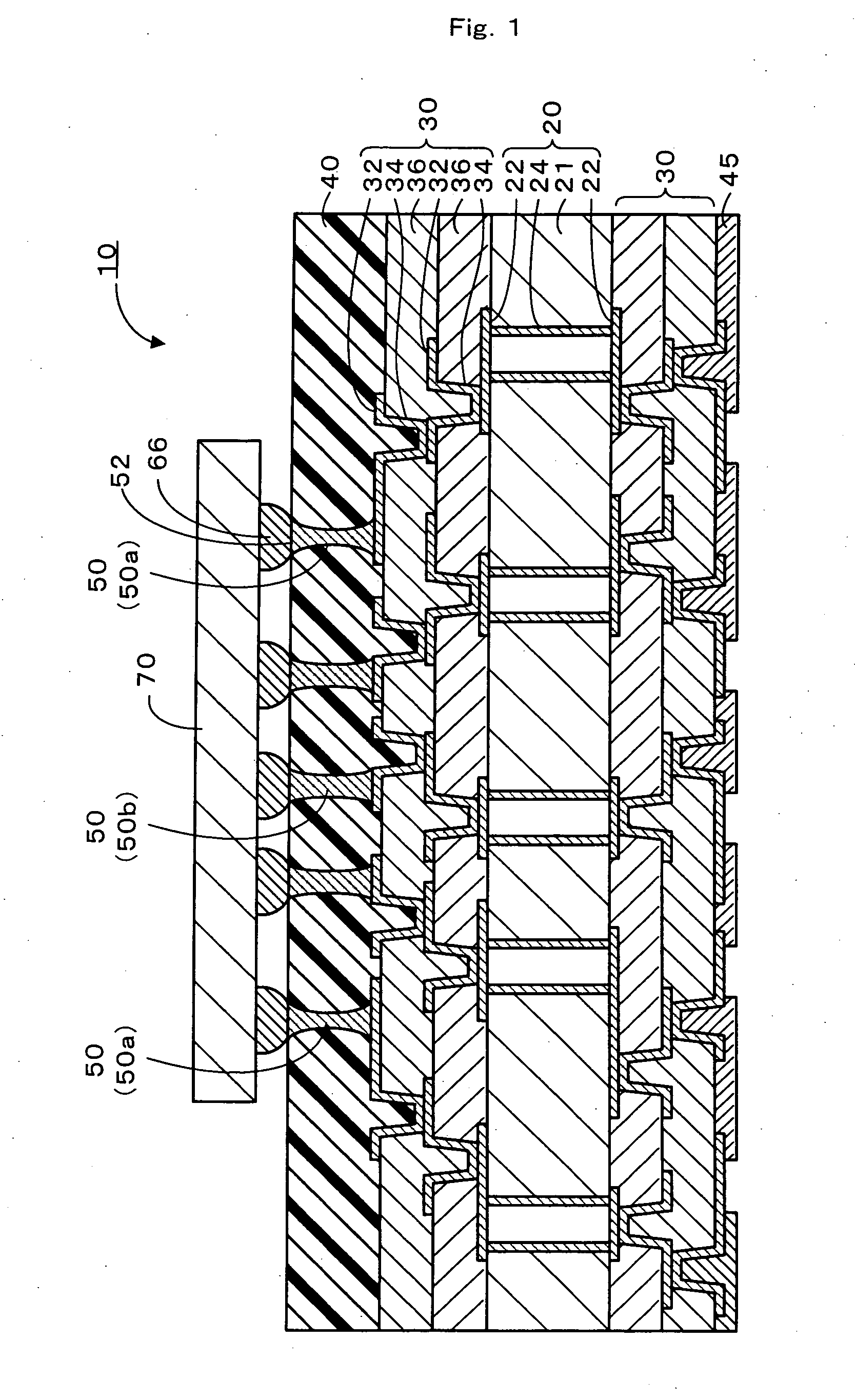
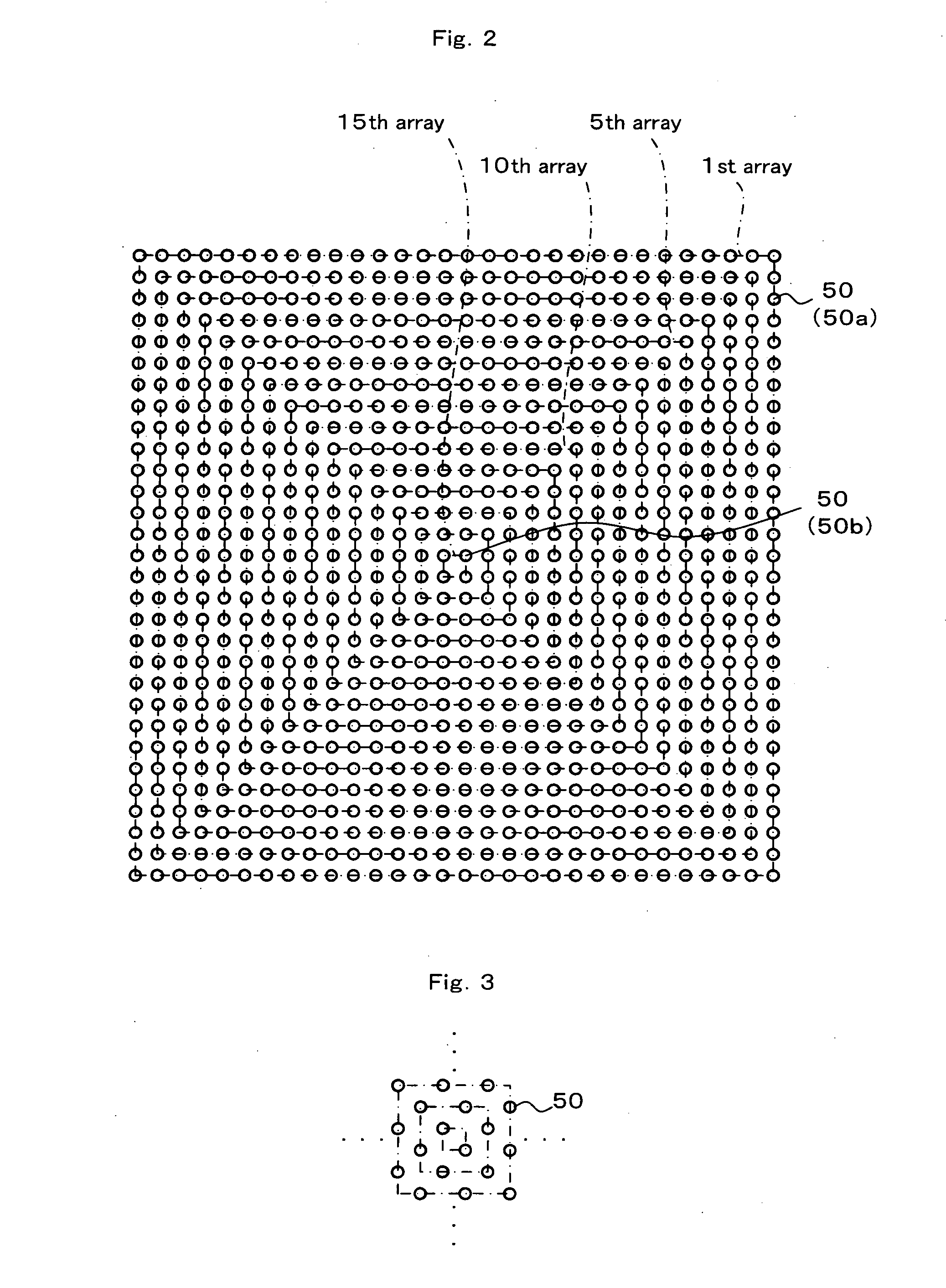
[0052] Examples for verifying the effects of the multilayer printed wiring board 10 of the embodiment shall now be described. First, the relationship between the aspect ratio Rasp of the conductor posts and the percentage variation of the electrical resistance after repeating heating and cooling shall be described. Multilayer printed wiring boards having conductor posts (30 by 30 square conductor posts are arranged in lattice-like manner, forming multiple arrays from an outermost array to a fifteenth array) of Examples 1 to 23, shown in Table 1, were prepared in accordance with the above embodiment. In Table 1, the multilayer printed wiring boards of Examples 1 to 12 have conductor posts, with which the minimum diameter and the maximum diameter are the same, that is, conductor posts having a substantially straight, columnar shape, and these examples were prepared in accordance with the preparation procedures shown in FIG. 7. The multilayer printed wiring boards of Examples 13 to 23 ...


PUM

PropertyMeasurementUnit
Temperatureaaaaaaaaaa
Pressureaaaaaaaaaa
Pressureaaaaaaaaaa

Abstract

A multilayer printed wiring board 10 includes: a build-up layer 30 that is formed on a core substrate 20 and has a conductor pattern 32 disposed on an upper surface; a low elastic modulus layer 40 that is formed on the build-up layer 30; lands 52 that are disposed on an upper surface of the low elastic modulus layer 40 and connected via solder bumps 66 to a IC chip 70; and conductor posts 50 that pass through the low elastic modulus layer 40 and electrically connect lands 52 with conductor patterns 32. The conductor posts 50 have the aspect ratio Rasp (height/minimum diameter) of not less than 4 and the minimum diameter exceeding 30 μm, and the aspect ratio Rasp of external conductor posts 50a, which are positioned at external portions of the low elastic modulus layer 40, is greater than or equal to the aspect ratio Rasp of internal conductor posts 50b, which are positioned at internal portions of the low elastic modulus layer 40.

Description

BACKGROUND OF THE INVENTION [0001] 1. Field of the Invention [0002] The present invention concerns a multilayer printed wiring board. [0003] 2. Description of the Prior Art [0004] Electronic equipment, as represented by portable information terminals and communication terminals, are being made remarkably high in function and compactness in recent years. As a form of achieving high-density mounting of an IC chip used for such electronic equipment, onto a multilayer printed wiring board, the flip-chip method, with which the IC chip is surface-mounted directly onto the multilayer printed wiring board, is employed. As such a multilayer printed wiring board, one known multilayer printed wiring board includes a core substrate, a build-up layer formed on the core substrate, and mounting electrodes by which a IC chip is mounted via solder bumps on an upper surface of the build-up layer. The core substrate used in such a multilayer printed wiring board is prepared by molding an epoxy resin, ...

Claims


Application Information

Patent Timeline
IPC IPC(8): H05K1/03H05K1/11H01L23/498H05K1/02H05K3/28H05K3/40H05K3/46
CPCH01L23/49811Y10T29/49162H01L23/49822H01L2224/16225H01L2924/01046H01L2924/01077H01L2924/01078H01L2924/01079H05K1/0271H05K3/28H05K3/4007H05K3/4602H05K2201/0133H05K2201/0367H05K2201/10674H01L2924/01019H05K1/0373H05K1/115H05K2201/068H01L2224/16235Y10T29/49151Y10T29/49126H01L23/49816H01L2924/00014H01L2924/00011H01L2224/0401H05K3/46
Inventor KARIYA, TAKASHIFURUTANI, TOSHIKI
Owner IBIDEN CO LTD
Why Eureka
Try Eureka