
Analytical scanning evanescent microwave microscope and control stage

a scanning evanescent microwave microscope and scanning evanescent technology, applied in material analysis using wave/particle radiation, instruments, nuclear engineering, etc., can solve the problems of unreliable test measurements, the tip of the probe used to measure the dielectric and conductivity properties of the test specimen often comes into contact, and the conductivity measurement cannot be accurately performed with a four-point prob

Inactive Publication Date: 2006-10-19
INTEMATIX
View PDF7 Cites 9 Cited by
  • Summary
  • Abstract
  • Description
  • Claims
  • Application Information

AI Technical Summary

Benefits of technology

[0008] The present invention also provides methods of fast data acquisition of resonant frequency and quality factor of a resonator; more specifically, the microwave resonator in a scanned evanescent microwave probe.

Problems solved by technology

Quantitative conductivity measurements of the test specimen can only be accurately performed with a four-point probe.
A drawback associated with performing the aforementioned measurements is that the probe tip used to measure the dielectric and conductivity properties of the test specimen often comes into contact with the test specimen.
Repeated contact between the probe tip and the test specimen causes damage to both the probe tip and the specimen, thereby making the resulting test measurements unreliable.
Another drawback associated with the aforementioned measurements is that gap distance between the probe tip and the test specimen can only be accurately controlled over a milli-meter (mm) distance range.

Method used


Image

  • Analytical scanning evanescent microwave microscope and control stage
  • Analytical scanning evanescent microwave microscope and control stage
  • Analytical scanning evanescent microwave microscope and control stage

Examples


embodiment a

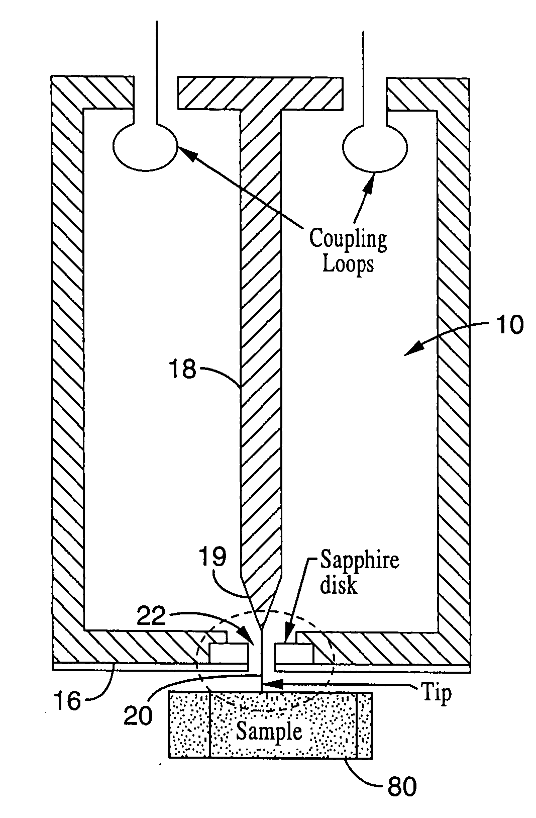
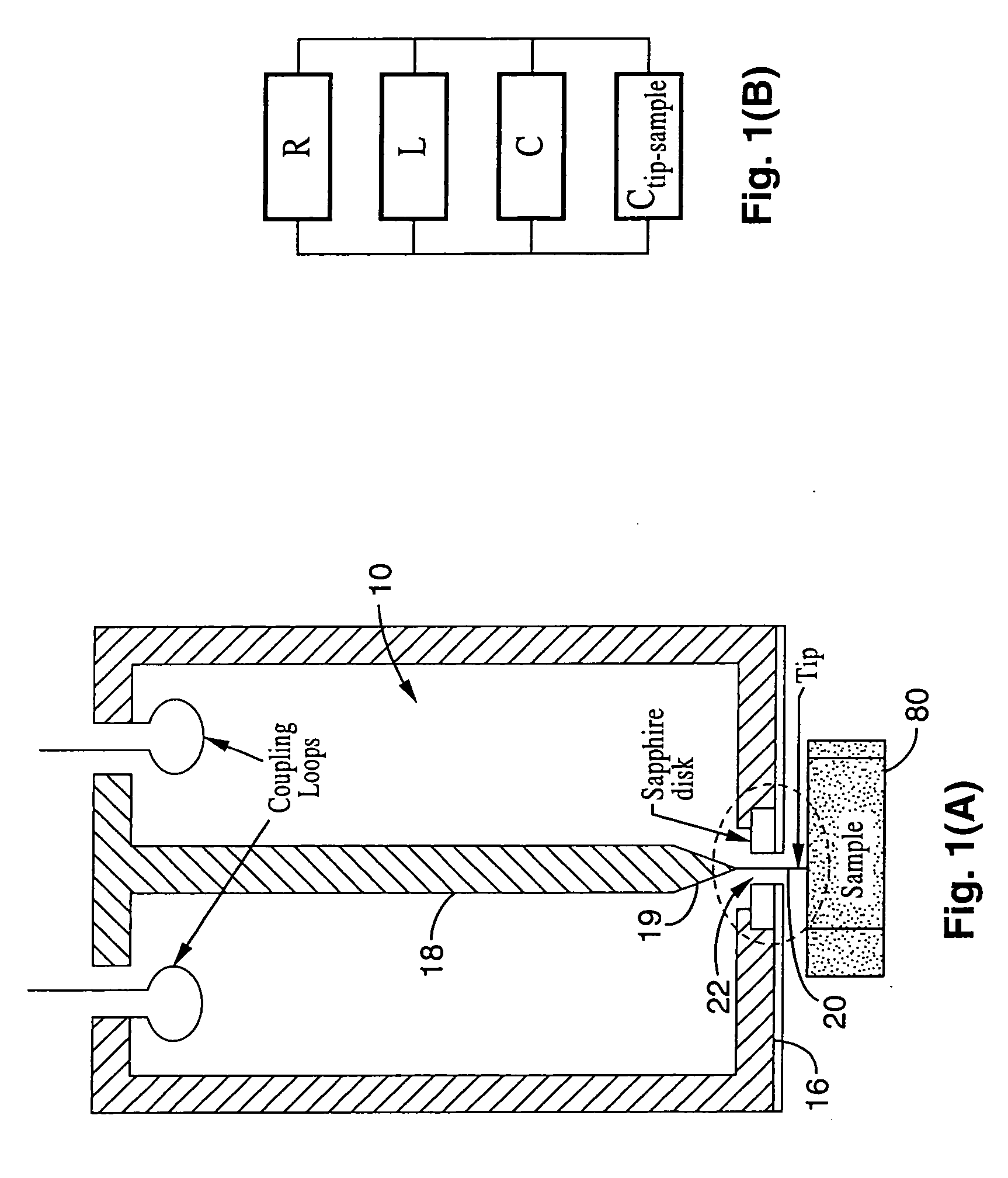
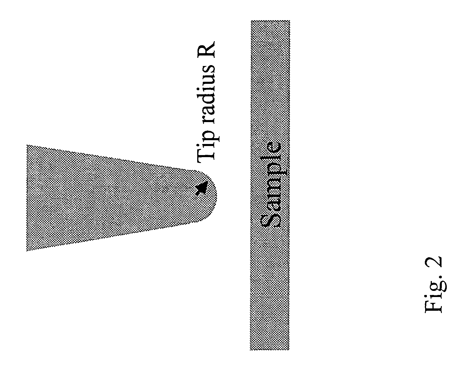
[0031] To determine quantitatively the physical properties, such as the complex dielectric constant, nonlinear dielectric constant and conductivity, through measurements of changes in resonant frequency (fr)and quality factor (Q) as function of different materials, bias electric and magnetic fields, tip-sample distance and temperature, etc. by a scanned evanescent microwave probe (SEMP), a quantitative model of the electric and magnetic fields in the tip-sample interaction region is necessary. A number of quasistatic models can be applied to the calculation of the probe response to dielectric, nonlinear dielectric and conductive materials. For the present invention, these models are applied to the calculation of the complex dielectric constant, nonlinear dielectric constant, and conductivity.

[0032] To determine the electrical properties of a sample, the variation in resonant frequency (fr) and quality factor (Q) of a resonant cavity is measured. (FIG. 1(A)). The tip-sample interact...

embodiment b

[0074] The above described models are applied to the regulation of the tip-sample separation for dielectric and conductive materials. In principle, with above models, the relationship between tip sample distance, electrical impedance and measured signals (fr and Q as function of sample difference, bias fields and other variables) is known precisely, at least when the tip is very close to the sample. If measured fr and Q signal points (and their derivatives with respect to electric or magnetic fields, distance and other variables) are more than unknown parameters, the unknowns can be uniquely solved. If both tip-sample distance and electrical impedance can be determined simultaneously, then the tip-sample distance can be easily controlled, so that the tip is always kept above the sample surface with a desired gap (from zero to microns). Both topographic and electrical impedance profiles can be obtained. The calculation can be easily performed by digital signal processor or any comput...

embodiment c

[0094] By contrast to most types of microscope, SEMM measures a complex quantity, i.e., the real and imaginary parts of the electrical impedance. This is realized by measuring the changes in the resonant frequency (fr) and quality factor (Q) of the resonator simultaneously. A conventional method of measuring these two quantities is to sweep the frequency of the microwave generator and measure the entire resonant curve. For each measurement, this can take seconds to minutes depending on the capabilities of the microwave generator. These measurements are limited by the switching speed of a typical microwave generator to roughly 20 Hz. With the use of a fast direct digital synthesizer based microwave source, the throughput can be improved to roughly 10 kHz, but is still limited by the need to switch over a range of frequencies. Another method is to implement an analog phase-locked loop for frequency feedback control. This method can track the changing resonant frequency in real time an...


PUM

PropertyMeasurementUnit
frequenciesaaaaaaaaaa
frequency sensitivityaaaaaaaaaa
electromagnetic propertyaaaaaaaaaa

Abstract

A scanning evanescent microwave microscope (SEMM) that uses near-field evanescent electromagnetic waves to probe sample properties is disclosed. The SEMM is capable of high resolution imaging and quantitative measurements of the electrical properties of the sample. The SEMM has the ability to map dielectric constant, loss tangent, conductivity, electrical impedance, and other electrical parameters of materials. Such properties are then used to provide distance control over a wide range, from to microns to nanometers, over dielectric and conductive samples for a scanned evanescent microwave probe, which enable quantitative non-contact and submicron spatial resolution topographic and electrical impedance profiling of dielectric, nonlinear dielectric and conductive materials. The invention also allows quantitative estimation of microwave impedance using signals obtained by the scanned evanescent microwave probe and quasistatic approximation modeling. The SEMM can be used to measure electrical properties of both dielectric and electrically conducting materials.

Description

[0001] This application claims benefit of provisional application Ser. No. 60 / 141,698 filed Jun. 30, 1999.[0002] This invention was made with U.S. Government support under Contract No. DE-AC03-76SF00098 between the U.S. Department of Energy and the University of California for the operation of Lawrence Berkeley Laboratory. The U.S. Government may have certain rights in this invention.FIELD OF THE INVENTION [0003] This invention relates generally to scanning probe microscopy and more specifically to scanning evanescent electromagnetic wave microscopy and / or spectroscopy. BACKGROUND OF THE INVENTION [0004] Quantitative dielectric measurements are currently performed by using deposited electrodes on large length scales (mm) or with a resonant cavity to measure the average dielectric constant of the specimen being tested. Quantitative conductivity measurements of the test specimen can only be accurately performed with a four-point probe. A drawback associated with performing the aforeme...

Claims


Application Information

Patent Timeline
Patent Type & Authority Applications(United States)
IPC IPC(8): G01N23/00
CPCB82Y20/00G01Q60/22B82Y35/00
Inventor XIANG, XIAO-DONGGAO, CHENDUEWER, FREDYANG, HAI TAO
Owner INTEMATIX
Learn More