Semicondustor device

a technology of semiconductor devices and circuit blocks, applied in electric devices, pulse techniques, instruments, etc., can solve problems such as increasing current (sub-threshold current), increasing power consumption in standby mode, etc., to achieve the effect of preventing malfunction in circuit blocks, improving reliability, and reducing area

Inactive Publication Date: 2006-10-19
RENESAS ELECTRONICS CORP
View PDF5 Cites 13 Cited by
  • Summary
  • Abstract
  • Description
  • Claims
  • Application Information

AI Technical Summary

Benefits of technology

[0016] A semiconductor device of the present invention has a power supply line (second power supply line) which is interrupted, a power supply line (first power supply line) which is not interrupted, and a voltage determination circuit for determining voltage level of the power supply line which is interrupted. With the configuration, when the interrupted power supply line is reset, after the voltage level of the power supply line is determined, operations of a circuit block connected to the power supply line can be restarted. Thus, without fear of malfunction, reliability improves.
[0017] A semiconductor device of the present invention has a plurality of power supply lines. In a configuration that at least one of the power supply lines can be interrupted, the power supply line which can be interrupted is driven by a regulator circuit. In such a configuration, the power supply is interrupted by stopping the regulator circuit (by making an output open) or fixing an output to the ground potential (ground voltage, reference source voltage). Consequently, the switch on the source voltage side and the switch on the ground potential side which are used in the conventional technique become unnecessary, so that the area can be reduced.
[0018] In this case, the semiconductor device may further include a voltage determining circuit for determining voltage level of a power supply line to be interrupted. On the basis of a determination result, a circuit block connected to the power supply line is enabled. In such a manner, as described above, malfunction in the circuit block can be prevented and reliability improves. By further providing the configuration with a power switch for connecting a plurality of power lines, the number of regulator circuits can be reduced and reliability of circuit operations can be improved.
[0019] Specifically, for example, in a case such that a standby regulator circuit for supplying power in a power saving mode, by turning on the power switch, the standby regulator circuit can be shared by the plurality of power supply lines. In some cases, a voltage determining circuit can be also shared. Also in a normal operation mode, by providing the power switch, the potentials of the power supply lines become the same with high precision. Thus, reliability of operations in the circuits improves.
[0020] In the case of such a configuration, at the time of interrupting a certain power supply line, it is necessary to turn off a desired power switch related to the power supply line. First, after turning off the power switch, the regulator circuit for interrupting power supply is turned off, and an output is grounded, so that voltage fluctuations in the power supply lines connected to each other by the power switch can be prevented and reliability improves. On the other hand, at the time of resetting the interrupted power supply line, first, the regulator circuit is started. After confirmation of rise in the voltage of the regulator circuit by the voltage determining circuit, the power switch is turned on. Simultaneously, the circuit block connected to the interrupted power supply line is enabled By such a sequence, voltage fluctuations in the interrupted power supply line and a power supply line connected by the power switch can be prevented. In addition, the circuit block connected to the interrupted power supply line can be operated without malfunction. Therefore, reliability can be improved.
[0021] Effects obtained by the representative ones of the inventions disclosed in the application will be briefly described. Power saving and improvement in reliability of the semiconductor device can be realized and reduction in the area of the semiconductor device can be realized.

Problems solved by technology

However, as the threshold voltage decreases, a leak current (sub-threshold current) increases in a state where the transistor is off.
Consequently, increase in power consumption in the standby mode is becoming an issue.

Method used


Image

  • Semicondustor device
  • Semicondustor device
  • Semicondustor device

Examples


Embodiment Construction

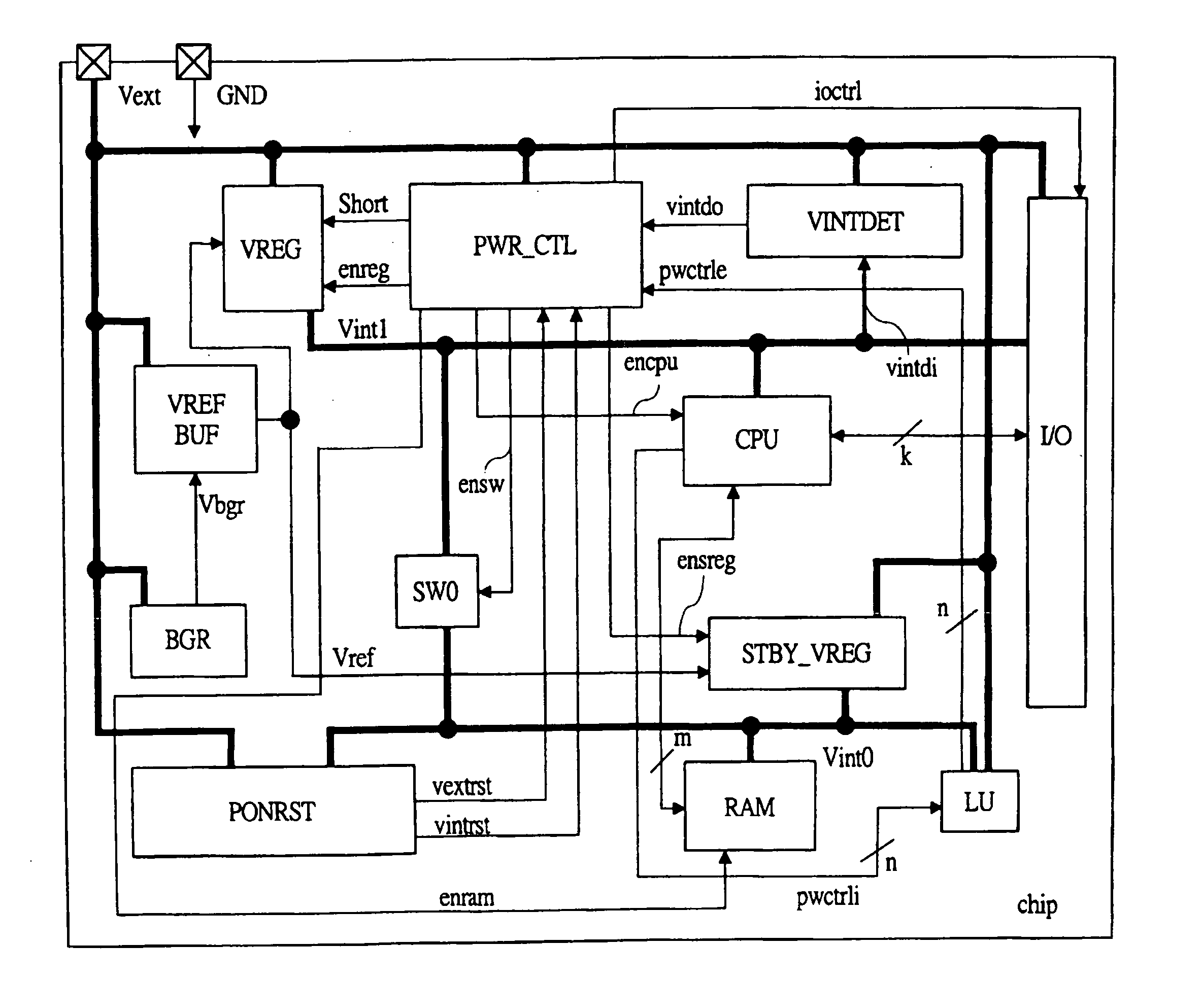
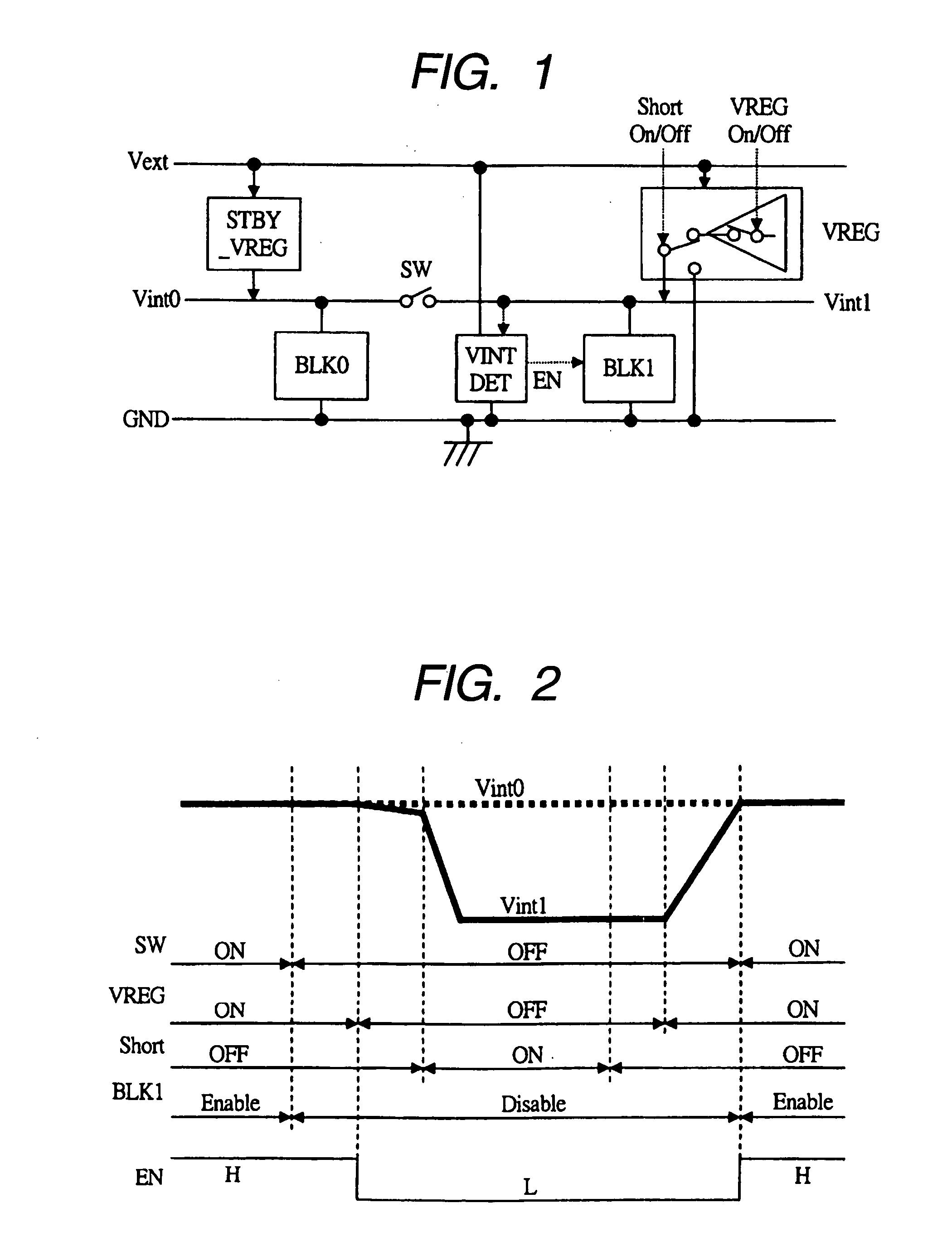
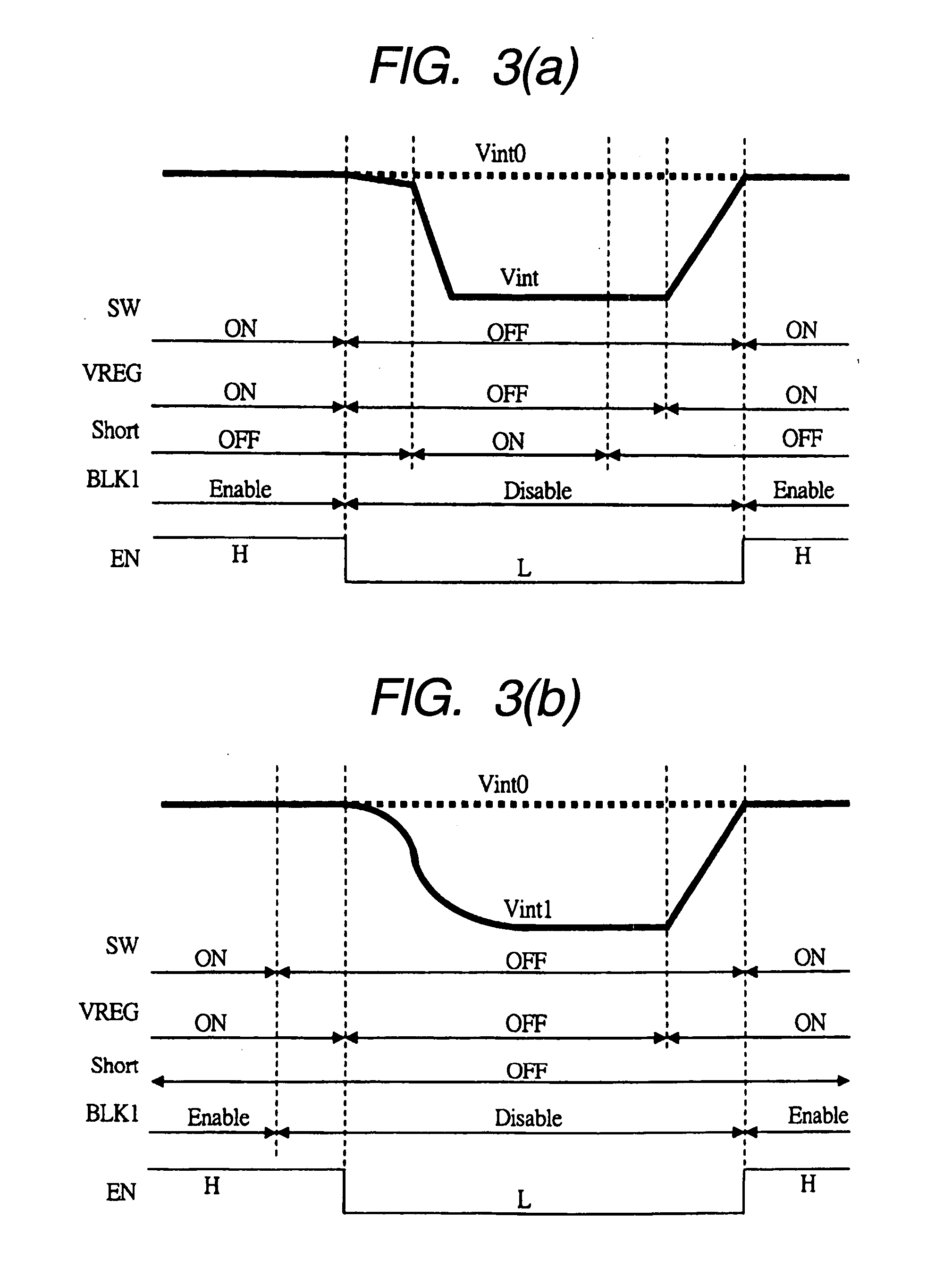
[0057] Embodiments of the present invention will be described in detail hereinbelow with reference to the drawings. In all of the diagrams for explaining the embodiments, as a rule, the same reference numerals are designated to the same member and their repetitive description will not be given. Circuit devices constructing each of the function blocks of the embodiment are, although not limited, formed on a semiconductor substrate made of single crystal silicon or the like by an integrated circuit technique of a known CMOS (complementary MOS) transistor or the like.

[0058] In the diagrams, by giving a symbol of circle to the gate of a PMOS transistor, the PMOS transistor is distinguished from an NMOS transistor. In the diagrams, in a portion in which connection of a substrate potential of a MOS transistor is not shown, the connecting method is not particularly limited as long as the MOS transistor can operate normally.

[0059] First, outline of main features of a semiconductor device ...


PUM


Abstract

The present invention provides a semiconductor device capable of realizing power saving and improvement in reliability or reduction in area. A semiconductor device includes: a power switch connecting an internal power supply in which power is not shut down and an internal power supply in which power is shut down; and an internal voltage determining circuit for determining voltage of the internal power supply in which power is shut down. Voltage of the internal power supply in which power is shut down is generated from voltage of an external power supply by using a regulator circuit. When the power of the internal power supply is interrupted, the power switch is turned off, the regulator circuit is turned off, and an output of the regulator circuit is shorted to a ground potential. When the power of the internal power supply is resumed, the regulator circuit is turned on, shorting is cancelled, the increased voltage of the internal power supply is determined by the internal voltage determining circuit, operation of a circuit block is started, and the switch is turned on.

Description

CROSS-REFERENCE TO RELATED APPLICATION [0001] The present application claims priority from Japanese patent application No. 2005-118290 filed on Apr. 15, 2005, the content of which is hereby incorporated by reference into this application. BACKGROUND OF THE INVENTION [0002] The present invention relates to a semiconductor device and, more particularly, to a technique effectively applied to a semiconductor device such as a microcomputer or a system LSI having a power shutoff function for reduction in power consumption. [0003] For example, Japanese Unexamined Patent Publication No. 2003-032399 discloses an image processor having a selection switch capable of switching a power to be supplied to a volatile memory between a main power supply or a standby power supply, and means for controlling the selection switch. The means for controlling the selection switch includes a main power supply level detector for detecting a voltage drop accompanying stop of the main power supply and switching...

Claims


Application Information

Patent Timeline
Patent Type & Authority Applications(United States)
IPC IPC(8): G06F19/00H03K19/00
CPCG06F1/3203Y02B60/1282Y02B60/1278G06F1/3287Y02D10/00
Inventor ITO, TAKAYASUHIRAKI, MITSURUHORIGUCHI, MASASHISHIMOGAWA, TOYOHIRO
Owner RENESAS ELECTRONICS CORP
Why Eureka
Try Eureka