NAND Flash Memory Device Having Dummy Memory cells and Methods of Operating Same

a memory device and dummy technology, applied in the field of semiconductor memory devices, can solve problems such as f-n tunneling, memory that loses stored data, and increased channel voltage of the program inhibiting cell, and achieve the effect of reducing the risk of leaking, and improving the efficiency of the program

Active Publication Date: 2006-10-26
SAMSUNG ELECTRONICS CO LTD
View PDF7 Cites 130 Cited by
  • Summary
  • Abstract
  • Description
  • Claims
  • Application Information

AI Technical Summary

Benefits of technology

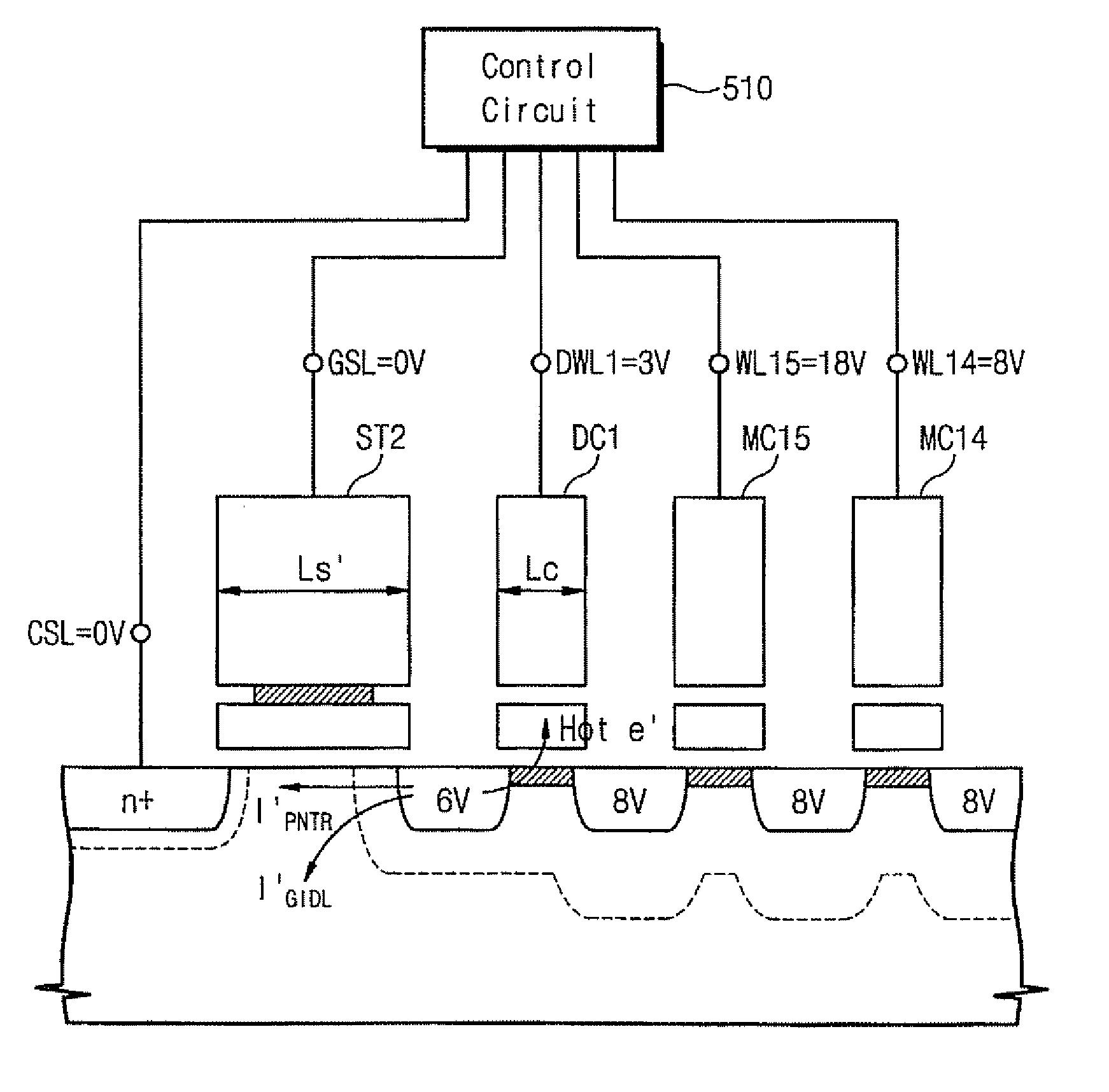
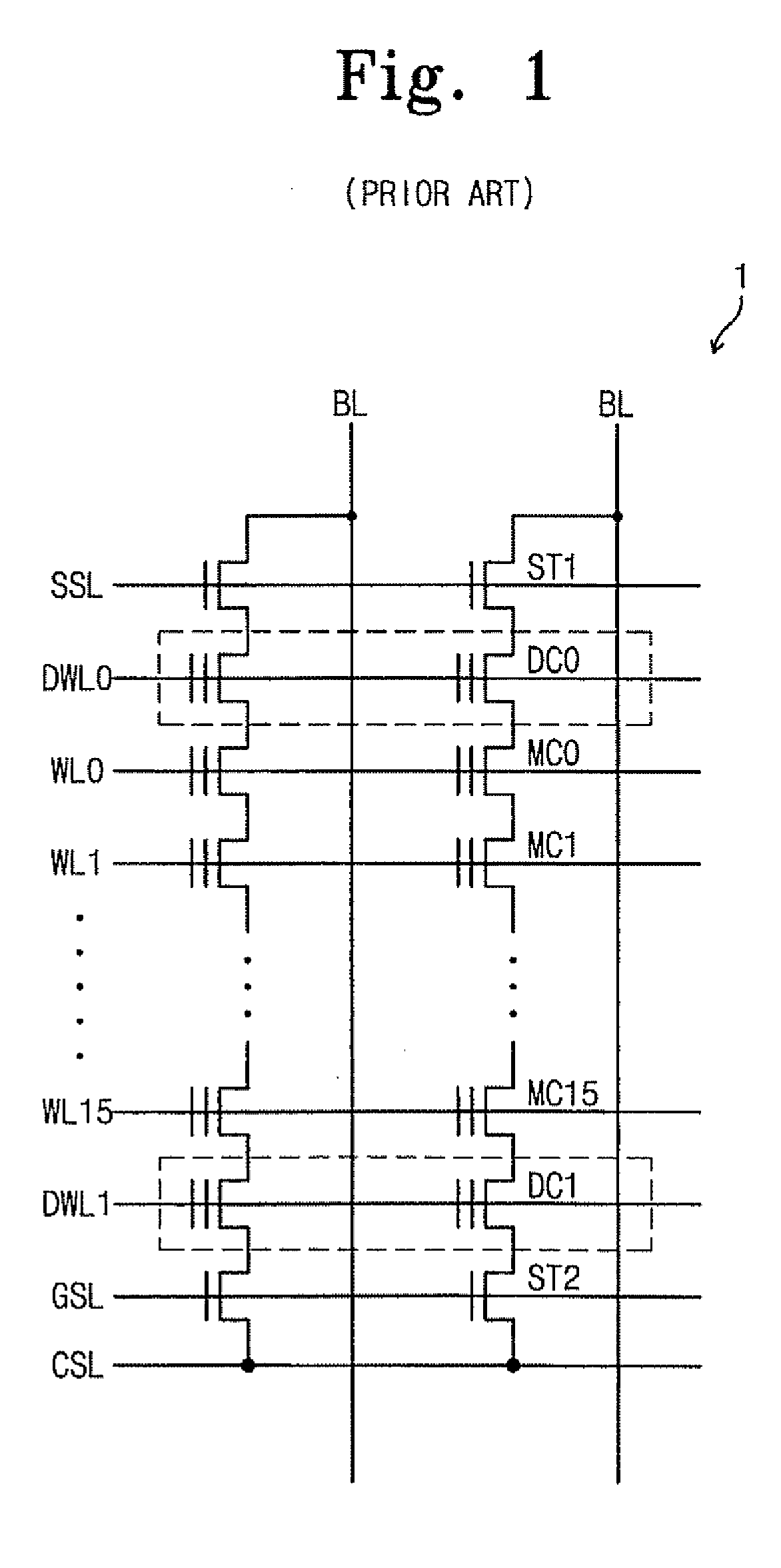
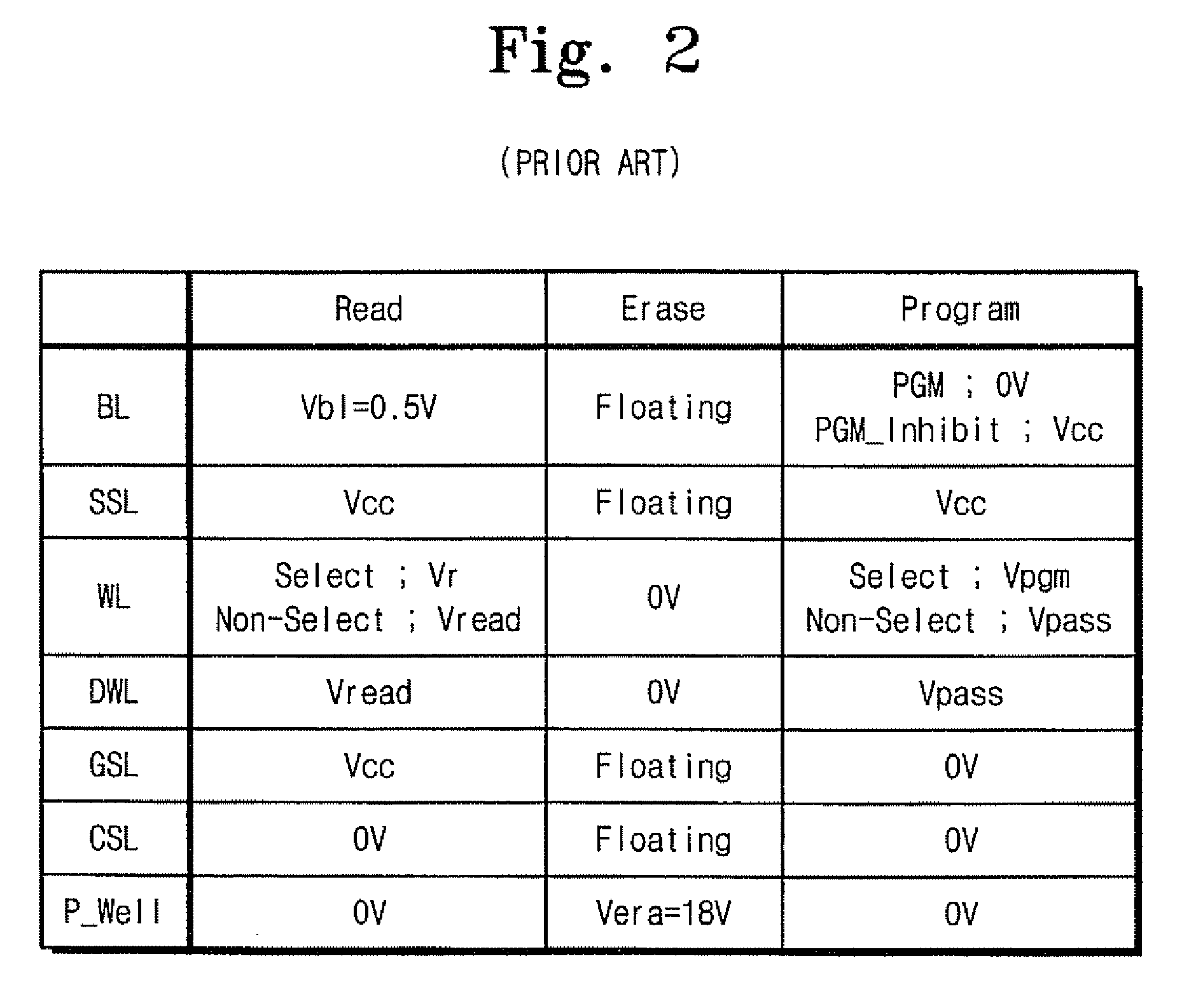
[0019] In some embodiments of the present invention, a NAND flash memory device includes a plurality of memory cells connected in series, at least one dummy memory cell connected in series with the plurality of memory cells, and a selection transistor connected in series with the dummy memory cell and the plurality of memory cells. The memory device further includes a control circuit configured to apply, during a program operation, a first word line voltage to non-selected ones of the memory cells, a second word line voltage greater than the first word line voltage to a selected memory cell, and a third word line voltage lower than the first word line voltage to the dummy memory cell. The selected memory cell may be a program inhibit cell. The selection transistor may be connected between the dummy memory cell and a bit line, and the control circuit is configured to apply a power supply voltage to the bit line. The selection transistor may be connected between the dummy memory cell and a common source line.
[0020] In further embodiments of the present invention, a NAND flash memory device includes a plurality of memory cells connected in series, at least one dummy memory cell connected in series with the plurality of memory cells, and a selection transistor connected in series with the dummy memory cell. The device further includes a control circuit configured to program the dummy memory cell before and/or after erase operations on the plurality of memory cells and the dummy memory cell. The control circuit may be configured to perform an erase verification operation after an erase operation on the plurality of memory cells and the dummy memory cell. The control circuit may be configured to apply, during the erase verification operation, a first erase verify voltage to the memory cells, and a second erase verify voltage greater than the first verify voltage to the dummy memory cell. The first erase verify voltage may be 0V, and the second erase verify voltage ma...

Problems solved by technology

RAM is volatile memory that loses stored data when power is interrupted.
However, the dummy memory cells DC0 and DC1 do not perform program and a read operations, that is, the dummy memory cells DC0 and DC1 are not used as a data storage elements.
However, the channel voltage of the inhibited cell increases to about 8V due to a capacitive boosting effect formed between the gate and the channel, that is, an insufficient electric field is generated between the g...

Method used


Image

  • NAND Flash Memory Device Having Dummy Memory cells and Methods of Operating Same
  • NAND Flash Memory Device Having Dummy Memory cells and Methods of Operating Same
  • NAND Flash Memory Device Having Dummy Memory cells and Methods of Operating Same

Examples


Embodiment Construction

[0034] The present invention will be described more fully hereinafter with reference to the accompanying drawings, in which embodiments of the invention are shown. However, this invention should not be construed as limited to the embodiments set forth herein. Rather, these embodiments are provided so that this disclosure will be thorough and complete, and will fully convey the scope of the invention to those skilled in the art. In the drawings, the thickness of layers and regions are exaggerated for clarity. Like numbers refer to like elements throughout. As used herein the term “and / or” includes any and all combinations of one or more of the associated listed items.

[0035] The terminology used herein is for the purpose of describing particular embodiments and is not intended to be limiting of the invention. As used herein, the singular forms “a”, “an” and “the” are intended to include the plural forms as well, unless the context clearly indicates otherwise. It will be further under...


PUM


Abstract

A NAND flash memory device includes a control circuit configured to apply, during a program operation, a first word line voltage to non-selected ones of a plurality of serially-connected memory cells, a second word line voltage greater than the first word line voltage to a selected one of the plurality of memory cells, and a third word line voltage lower than the first word line voltage to a dummy memory cell connected in series with the plurality of memory cells. In other embodiments, a control circuit is configured to program a dummy memory cell before and/or after each erase operation on a plurality of memory cells connected in series therewith. In still other embodiments, a control circuit is configured to forego erasure of a dummy memory cell while erasing a plurality of memory cells connected in series therewith.

Description

CROSS-REFERENCE TO RELATED APPLICATION [0001] This application claims the benefit of Korean Patent Application No. 2005-0032829, filed Apr. 20, 2005, and Korean Patent Application No. 2006-0027595, filed Mar. 17, 2006, the contents of which are hereby incorporated herein by reference in their entirety. BACKGROUND OF THE INVENTION [0002] The present invention relates to semiconductor memory devices, and more particularly, to NAND flash memory devices. [0003] Generally, a semiconductor memory device is a memory device for storing data and retrieving target data by reading stored data. Semiconductor memory devices may be classified as random access memory (RAM) and read only memory (ROM). RAM is volatile memory that loses stored data when power is interrupted. ROM is nonvolatile memory that holds stored data even when power is interrupted. RAM includes dynamic RAM and a static RAM. ROM includes programmable ROM, erasable ROM, electrically programmable ROM (EPROM), and flash memory. Fla...

Claims


Application Information

Patent Timeline
IPC IPC(8): G11C16/04G11C11/34
CPCG11C16/0483G11C16/3445G11C16/12G11C16/107
Inventor PARK, KI-TAECHOI, JUNG-DALSEL, JONG-SUNSHIN, YOO-CHEOL
Owner SAMSUNG ELECTRONICS CO LTD
Why Eureka
Try Eureka