Method and apparatus for crystallizing silicon, method of forming a thin film transistor, a thin film transistor and a display apparatus using same

a technology of amorphous silicon and thin film transistor, which is applied in the direction of crystal growth process, polycrystalline material growth, manufacturing tools, etc., can solve the problems of deteriorating the display quality of the display apparatus having the amorphous silicon thin film transistor, and achieve the effect of reducing the load reducing the output energy, and increasing the lifetime of the apparatus for generating the laser beam

Inactive Publication Date: 2006-10-26
SAMSUNG ELECTRONICS CO LTD
View PDF7 Cites 2 Cited by
  • Summary
  • Abstract
  • Description
  • Claims
  • Application Information

AI Technical Summary

Benefits of technology

[0026] A laser beam having the decreased output energy is irradiated on the amorphous silicon thin film to crystallize the amorphous silicon thin film to a polysilicon thin film so that the load of the apparatus of generating the laser beam is decreased, and the lifetime of the apparatus for generating the laser beam increases. In addition, the characteristics of the thin film transistor and the display quality of the display apparatus is improved.

Problems solved by technology

Therefore, display quality of the display apparatus having the amorphous silicon thin film transistor may be deteriorated.

Method used


Image

  • Method and apparatus for crystallizing silicon, method of forming a thin film transistor, a thin film transistor and a display apparatus using same
  • Method and apparatus for crystallizing silicon, method of forming a thin film transistor, a thin film transistor and a display apparatus using same
  • Method and apparatus for crystallizing silicon, method of forming a thin film transistor, a thin film transistor and a display apparatus using same

Examples


Embodiment Construction

[0040] Preferred embodiments of the present invention will now be described more fully hereinafter below with reference to the accompanying drawings. This invention may, however, be embodied in different forms and should not be construed as limited to the embodiments set forth herein. Rather, these embodiments are provided so that this disclosure will be thorough and complete, and will fully convey the scope of the invention to those skilled in the art.

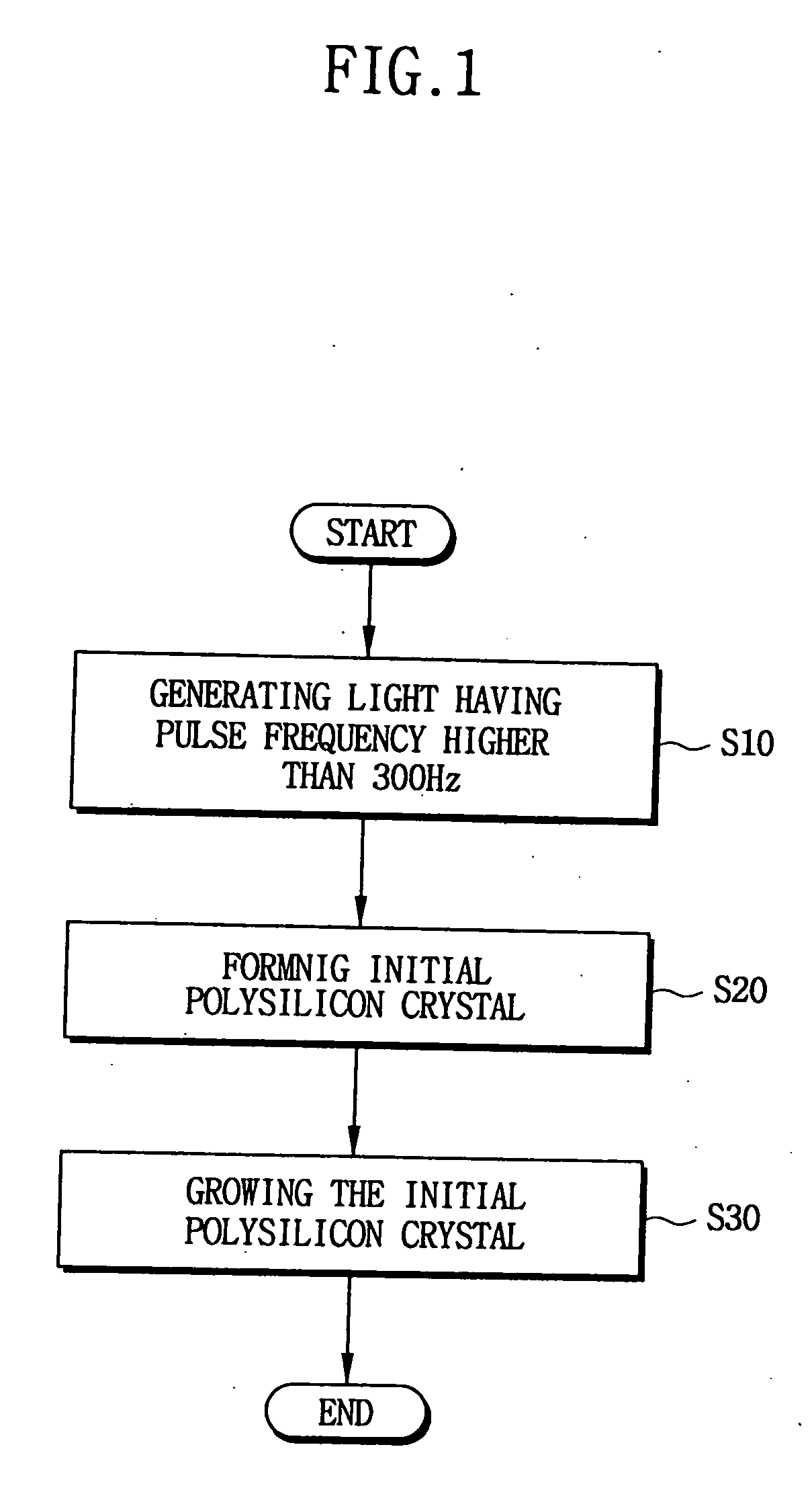
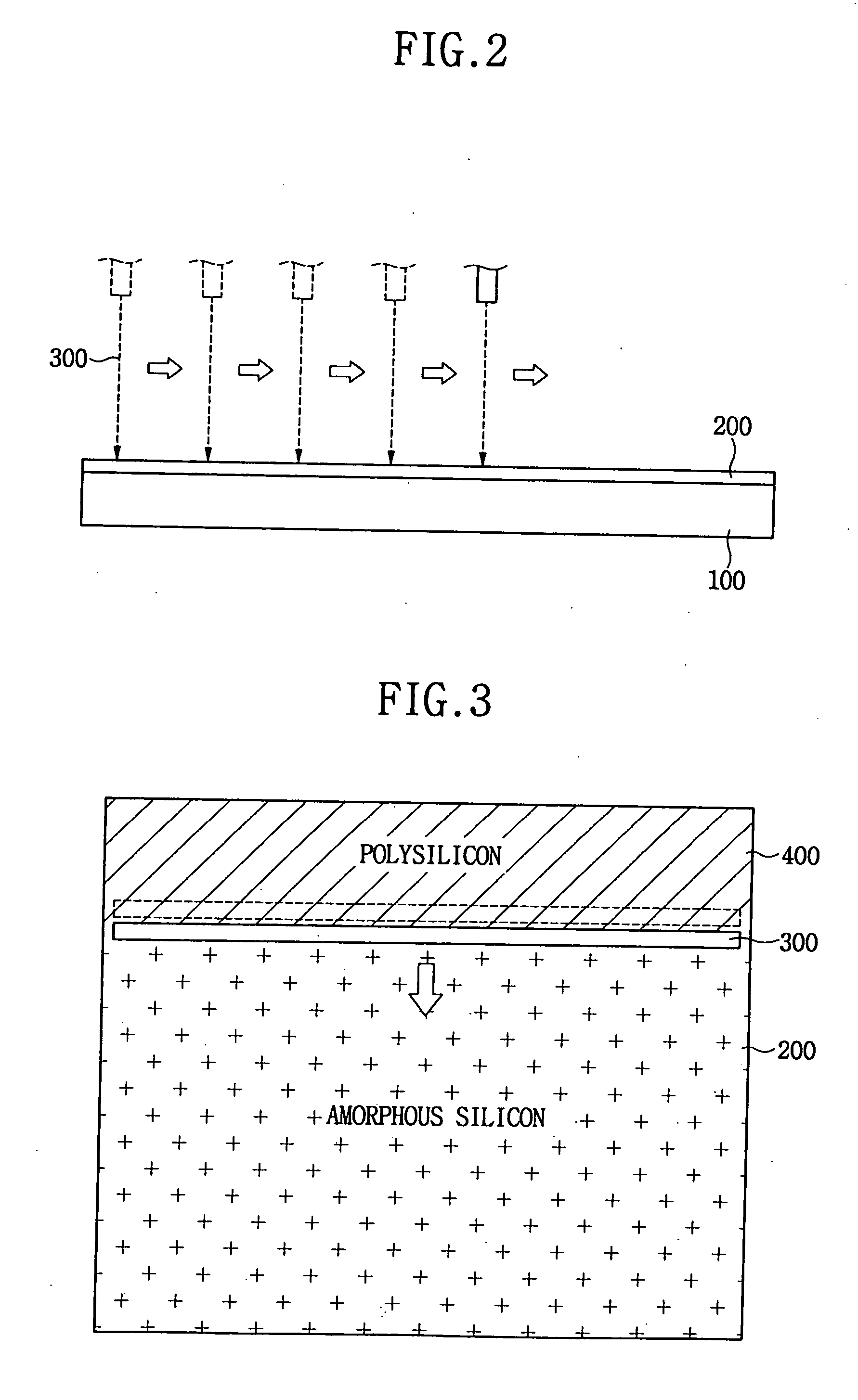
[0041]FIG. 1 is a flow chart showing a method of crystallizing silicon in accordance with an embodiment of the present invention. FIG. 2 is a cross-sectional view showing a silicon crystallizing process in accordance with an embodiment of the present invention.

[0042] Referring to FIGS. 1 and 2, an amorphous silicon thin film 200 is formed on a substrate 100.

[0043] In order to crystallize the amorphous silicon thin film 200 to a polysilicon thin film, light having a pulse frequency higher than about 300 Hz is generated (Step S10). T...


PUM

PropertyMeasurementUnit
frequencyaaaaaaaaaa
frequencyaaaaaaaaaa
output energyaaaaaaaaaa

Abstract

A light having a pulse frequency higher than about 300 Hz is generated. The light is irradiated on an amorphous silicon thin film for a predetermined time period to form an initial polysilicon crystal. The light is transported in a predetermined direction to grow the initial polysilicon crystal. A laser beam having a decreased output energy is irradiated on the amorphous silicon thin film to crystallize the amorphous silicon thin film to a polysilicon thin film so that the load of an apparatus for generating the laser beam is decreased, and the lifetime of the apparatus for generating the laser beam increases.

Description

CROSS-REFERENCE TO RELATED APPLICATION [0001] This application is a Continuation of U.S. application Ser. No. 10 / 844,998 filed on May 13, 2004, the entirety of which is fully incorporated herein by reference.BACKGROUND OF THE INVENTION [0002] 1. Technical Field [0003] The present disclosure relates to a method of crystallizing silicon, an apparatus for crystallizing silicon, a method of forming a thin film transistor using the method of crystallizing silicon, a thin film transistor and a display apparatus using same. [0004] 2. Discussion of the Related Art [0005] Display apparatuses that convert data in the form of an electric signal to an image are known. The data may be generated from an information processing device such as a computer. [0006] Display apparatuses, include, for example, cathode ray tube (CRT) display apparatuses or flat display apparatuses. [0007] Flat display apparatuses include, for example, liquid crystal display (LCD) apparatuses, plasma display panel (PDP) dis...

Claims


Application Information

Patent Timeline
Patent Type & Authority Applications(United States)
IPC IPC(8): H01L21/84H01L21/00H01L21/324B23K26/06B23K26/067B23K26/073C30B29/06C30B30/00C30B35/00H01L21/20H01L21/336H01L29/04H01L29/786
CPCB23K26/063B23K26/067B23K26/0673H01L29/78678B23K26/0736H01L21/2026H01L29/66765B23K26/0732B23K26/0622H01L21/02686H01L21/02678H01L21/02532H01L21/02691H01L21/324H01L21/02595
Inventor KIM, DONG-BYUMCHUNG, SE-JINCHUNG, UI-JIN
Owner SAMSUNG ELECTRONICS CO LTD
Why Eureka
Try Eureka