Structure of polymer-matrix conductive film and method for fabricating the same

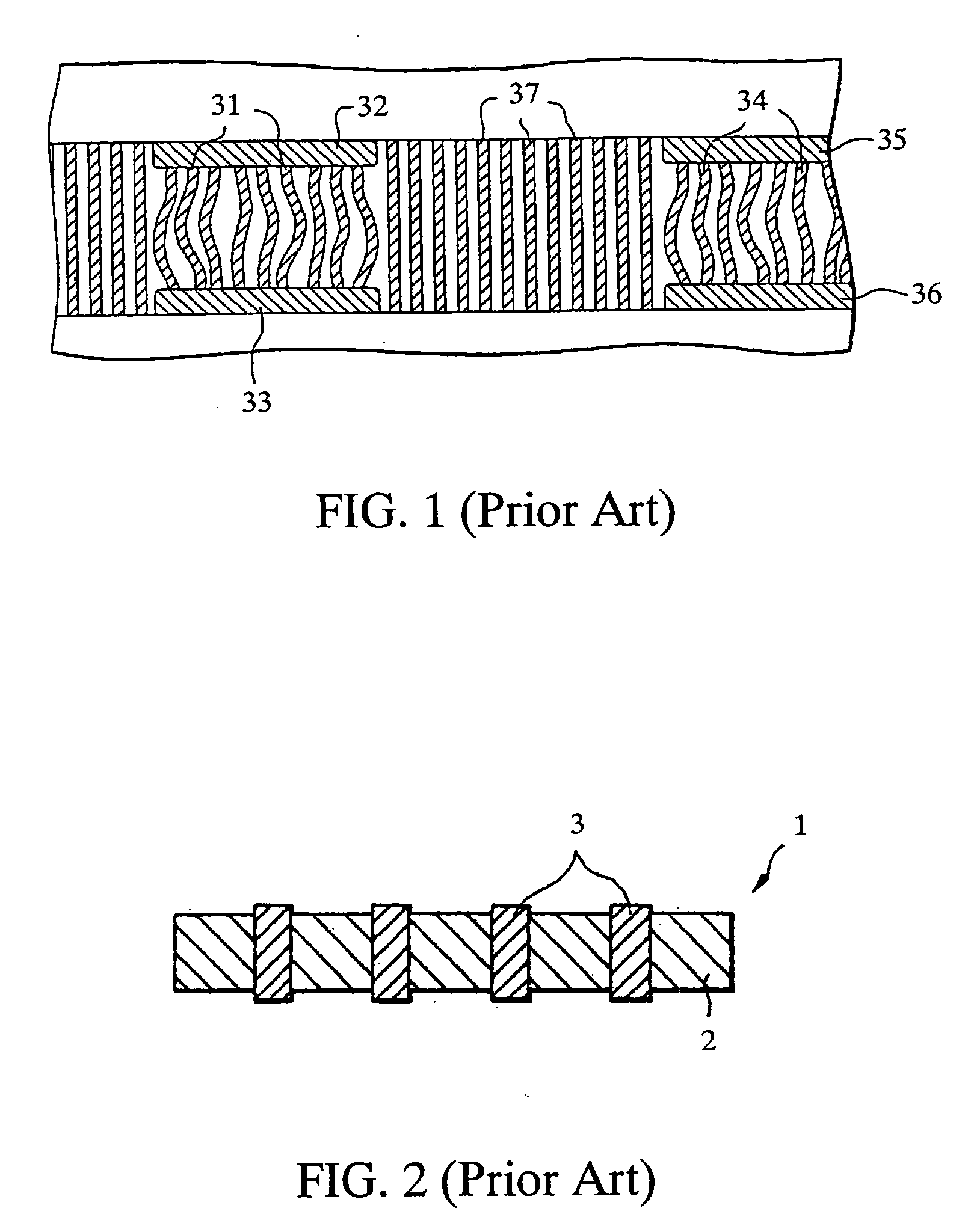
a technology of polymer matrix and conductive film, which is applied in the direction of nanoinformatics, semiconductor/solid-state device details, coupling device connections, etc., can solve the problems of z-axis conductive film not being used in flip-chip packages of less than 30 m pitch, size cannot be reduced further,

Inactive Publication Date: 2006-11-02
IND TECH RES INST
View PDF10 Cites 10 Cited by
  • Summary
  • Abstract
  • Description
  • Claims
  • Application Information

AI Technical Summary

Benefits of technology

[0011] A second objective of the present invention is to provide a sandwiched polymer-matrix conductive film and a method for fabricating the same, which can provide a Z-axis conductive film with a larger adhesive area to strengthen the package of a semiconductor device.
[0012] A third objective of the present invention is to provide a structure of anisotropic polymer-matrix conductive film and a method for fabricating the same, which can provide an input / output redistribution function in order that the current substrate can be applied to a package of fine-pitched chip in the future.
[0014] A larger adhering area is provided between the chip and the substrate by the sandwiched polymer-matrix conductive film. The portions of the chip and the substrate, except for their electrodes, are jointed with the polymer-matrix conductive film by the adhesive layer so as to enhance the package strength of the semiconductor device.
[0016] The present method can manufacture a composite conductive film having a polymer matrix and a plurality of conductive lines less than nanometers formed therein, which is suitable for electrical connection between the chip and the substrate with fine pitches.

Problems solved by technology

However, Z-axis conductive film cannot be used in a flip-chip package with pitch smaller than 30 μm because the size of the conductive particles in Z-axis conductive film is approximately 3 μm, and this size cannot be reduced any further.
As a result, Z-axis conductive film cannot be used in the flip-chip package of the pitch less than 30 μm.
Hence, Z-axis conductive film is not suitable for integrated circuit devices driven by current.
But the density of the conductive particles in conventional Z-axis conductive film is not very high for the purpose of maintaining insulation in X and Y directions (i.e. avoiding lateral short circuits).
Since the coefficients of thermal expansion (CTE) of the chip and substrate are mismatched, the stress there between adversely influences the reliability of the connection of the chip and the substrate.
However, when the jointing pitch is reduced to a size of less than 100 μm, the underfill does not easily enter the space between the chip and the substrate.
However, the above methods have disadvantages.
The Young's modulus of the copper stud is larger than that of the solder bump, and is a poor stress buffer.
Therefore, the conductive polymer is not suitable for electrical connection of the flip-chip package with fine pitches and small electrode areas.
The above method is costly and time-consuming.
Moreover, the uniformity of the pore diameters is not easily controlled.
Since the pores of the polymer film are previously formed, the polymer film cannot be a B-stage polymer.
Thus, the polymer film cannot provide sufficient adhesion during a subsequent jointing step by thermal press to maintain contact between the electrodes of the chip and the substrate and metal nanowires.
Thus, the reliability of electrical connection of the composite polymer film is degraded.
However, this manufacturing method is limited to the capability of a photolithographic process, and can merely manufacture metal wires with a diameter of 20 μm or more.
Alumina has good heat-dissipation and insulating properties, but its Young's modulus is too large and too fragile to release stress generated during packaging.
Moreover, the adhesion between alumina and the substrate, as well as between alumina and the chip is insufficient to maintain electrical connection of the electrodes and the conductive film.

Method used


Image

  • Structure of polymer-matrix conductive film and method for fabricating the same
  • Structure of polymer-matrix conductive film and method for fabricating the same
  • Structure of polymer-matrix conductive film and method for fabricating the same

Examples


Embodiment Construction

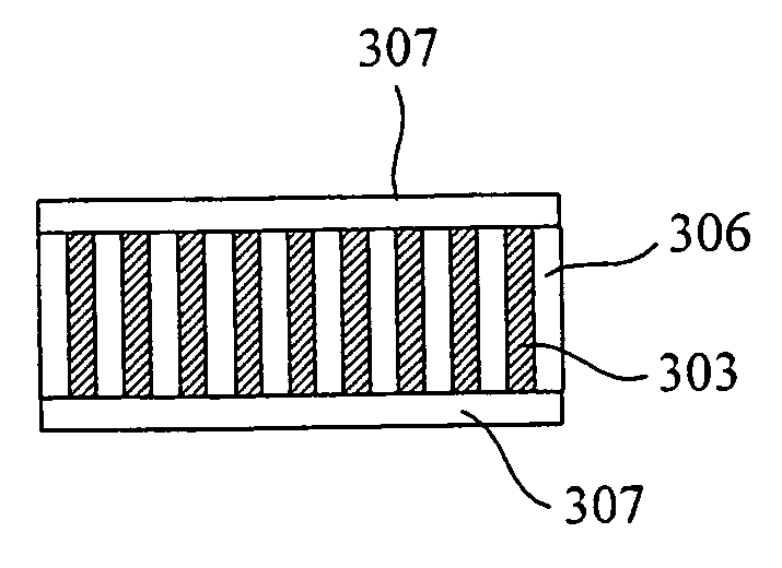
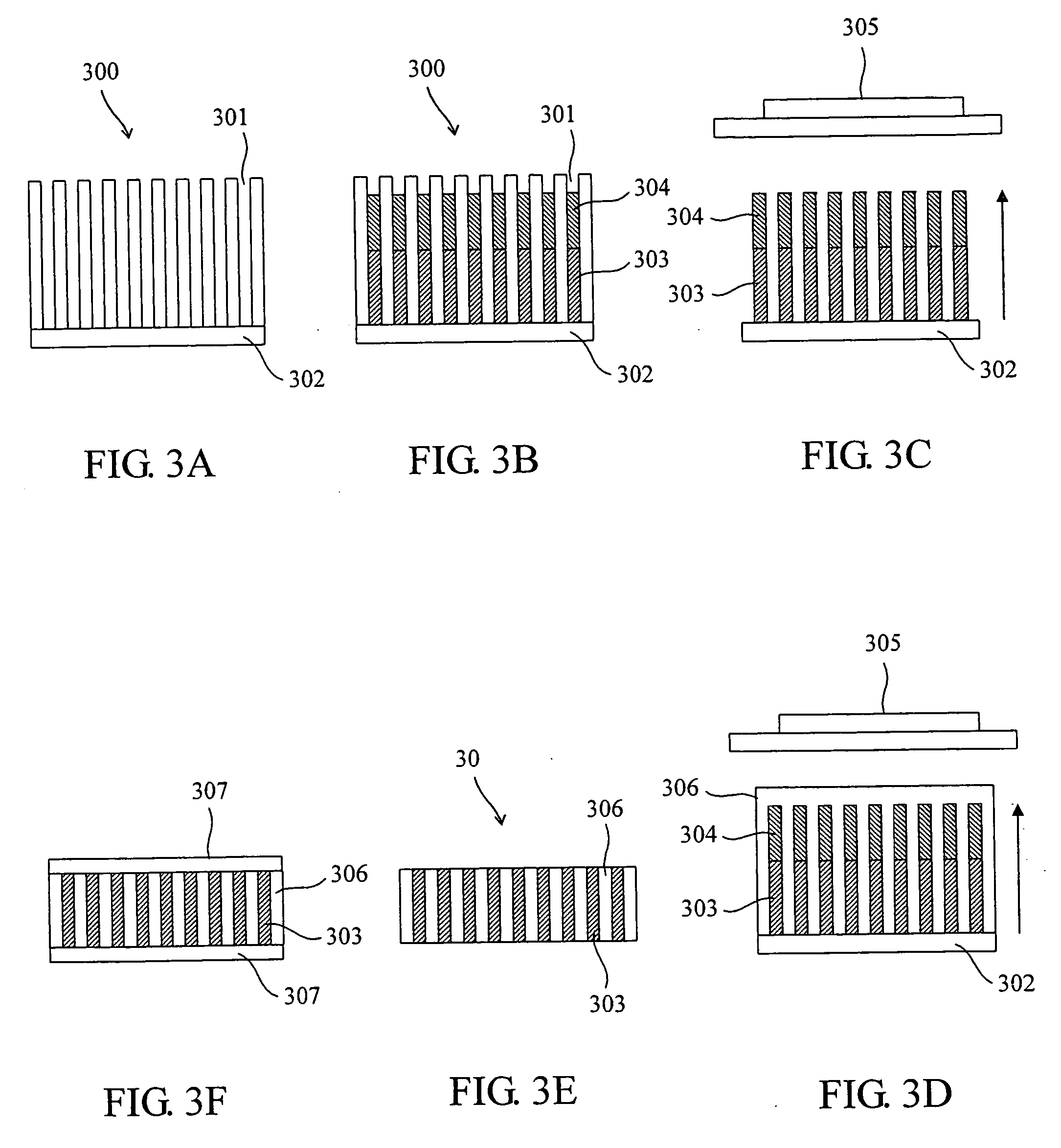
[0028] The present invention provides a universal Z-axis conductive film, which comprises a polymer matrix and a plurality of conductive lines less than micro-sized. The present Z-axis conductive film is suitable for a package of a semiconductor device in 45 nm technology node. The polymer matrix can be made of a material with a low Young's modulus to aid as a stress buffer during the subsequent packaging of the semiconductor device. In addition, the structure and composition of the conductive lines can be varied such that the present Z-axis conductive film can connect electrically with the chip and the substrate by bonding. The jointing resistance can thus be lowered.

[0029] However, it is necessary to keep Z-direction parallel of the conductive lines so as to maintain good insulation of the present Z-axis conductive film in X-Y directions. However, the diameter of the currently-used conductive lines is approximately 200 nm (nanometers) or less and their length is 10 μm (micrometer...


PUM

PropertyMeasurementUnit
sizeaaaaaaaaaa
sizeaaaaaaaaaa
sizeaaaaaaaaaa

Abstract

A composite conductive film formed of a polymer-matrix and a plurality of conductive lines less than micro-sized and its fabricating method are provided. The conductive lines are arranged parallel and spaced apart from each other so as to provide anisotropic conductivity. The present conductive film can serve as an electrical connection between a fine-pitch chip and a substrate. Additionally, an adhesive layer is formed on two opposite sides of the conductive film along its conductive direction to increase adhesive areas. The strength and reliability of the package using the conductive film are thus enhanced.

Description

BACKGROUND OF THE INVENTION [0001] 1. Field of the Invention [0002] The present invention relates to a Z-axis conductive film and a method for fabricating the same, and more particularly, the present invention relates to a composite conductive film including a polymer matrix and conductive nanowires and a method for fabricating the same. [0003] 2. Description of the Related Art [0004] Interconnection technology of a flip-chip package for the I / O pitch less than 50 μm (micrometer) is accomplished by Z-axis conductive films. However, Z-axis conductive film cannot be used in a flip-chip package with pitch smaller than 30 μm because the size of the conductive particles in Z-axis conductive film is approximately 3 μm, and this size cannot be reduced any further. As a result, Z-axis conductive film cannot be used in the flip-chip package of the pitch less than 30 μm. The electrical conduction of Z-axis conductive film is realized by contact between metallic films chemically electroplated ...

Claims


Application Information

Patent Timeline
Patent Type & Authority Applications(United States)
IPC IPC(8): H01L29/08
CPCB82Y10/00Y10T29/49204H01L24/83H01L2224/838H01L2924/01005H01L2924/01013H01L2924/01027H01L2924/01029H01L2924/01047H01L2924/01079H01L2924/0781H01L2924/12044H01L2924/14H01R4/04H01R13/2414H05K3/323H05K2201/026H05K2201/083H05K2201/10378H05K2203/0726H05K2203/104H01L24/29H01L2224/2919H01L2224/29298H01L2924/01006H01L2924/01033H01L2924/014H01L2924/0665H01L23/49827Y10T29/49126Y10T29/49155H01L2924/00013Y10S977/766Y10S977/77Y10S977/761Y10S977/778Y10S977/762H01L2924/00014H01L2924/00H01L2224/29099H01L2224/29199H01L2224/29299H01L2224/2929
Inventor UANG, RUOH-HUEYCHEN, YU-CHIHLIN, REN-JANCHENG, SYH-YUH
Owner IND TECH RES INST
Why Eureka
Try Eureka