Contact metallization scheme using a barrier layer over a silicide layer

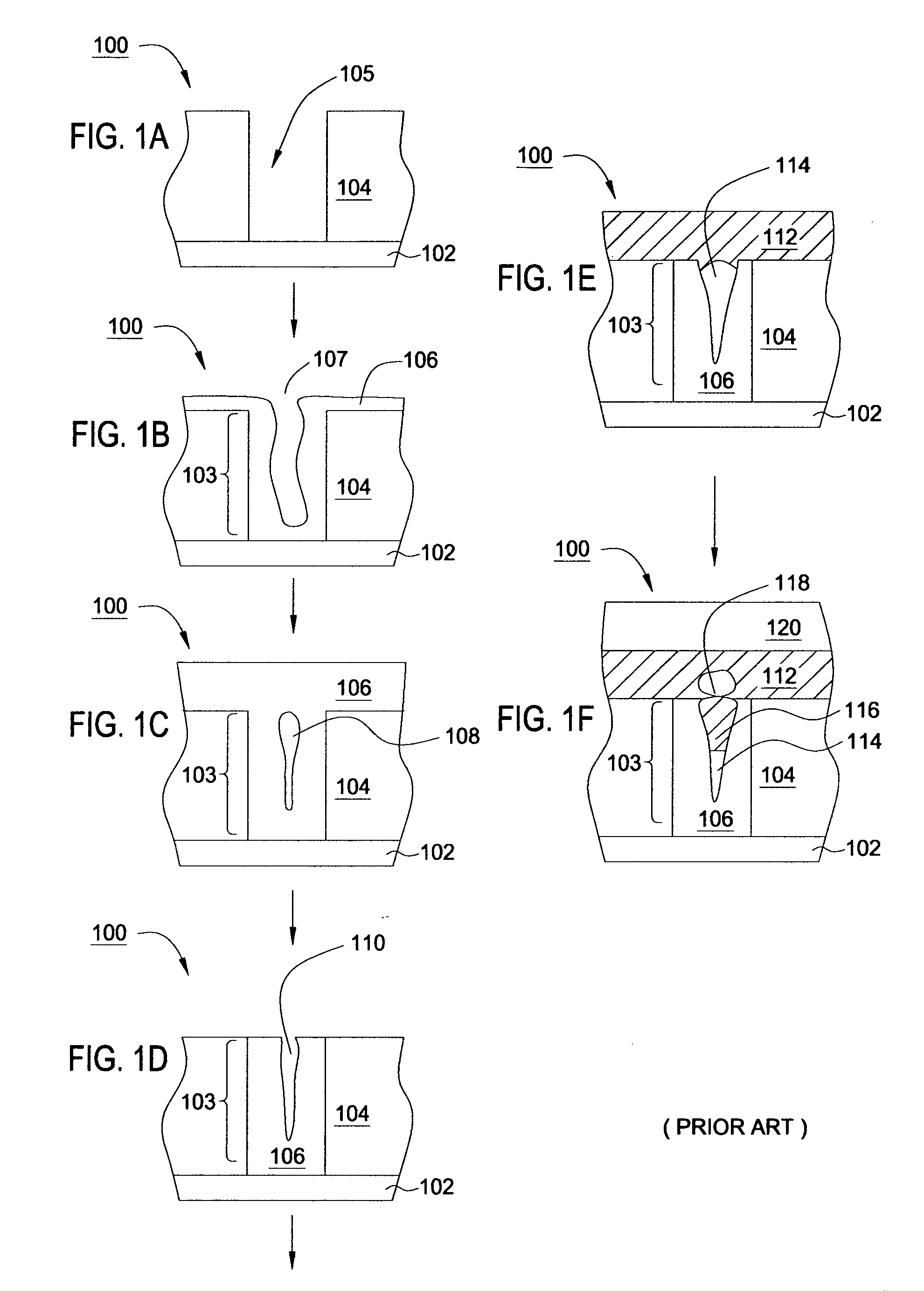
a technology of contact metallization and barrier layer, which is applied in the direction of resistive material coating, chemical vapor deposition coating, solid-state device, etc., can solve the problems of displacement of voids from one layer to the next, large amount of ongoing effort being directed, and the vapor deposition process for tungsten depositing suffers from void or seam type defect creation within the contact plug

Active Publication Date: 2006-11-09
APPLIED MATERIALS INC
View PDF99 Cites 327 Cited by
  • Summary
  • Abstract
  • Description
  • Claims
  • Application Information

AI Technical Summary

Benefits of technology

[0013] The present invention generally provide a method for depositing a material on a contact level feature formed on a substrate, comprising providing a substrate that has one or more contact level features that have an exposed silicide layer formed on a silicon containing region, depositing a barrier layer over the surface of the exposed silicide layer, wherein the depositing the barrier layer comprises depositing a first metal layer on the exposed silicide layer, and depositing a second metal layer over the first metal layer, wherein the second metal layer contains a metal selected from a group consisting of ruthenium (Ru), cobalt (Co), nickel (Ni), rhodium (Rh), iridium (Ir), palladium (Pd) and platinum (Pt), and filling the contact level feature with a metal containing layer.
[0014] Embodiments of the invention further provide a material on a contact level feature formed on a substrate, comprising providing a substrate that has one or more contact level features that have an exposed silicide layer formed on a doped silicon containing region, depositing a barrier layer over the surface of the exposed silicide layer, wherein the depositing the barrier layer comprises depositing a first metal layer on the exposed silicide layer, and depositing a second metal layer over the first metal layer, wherein the second metal layer contains a metal selected from a group consisting of ruthenium (Ru), cobalt (Co), nickel (Ni), rhodium (Rh), iridium (Ir), palladium (Pd) and platinum (Pt), electrolessly depositing a first copper containing layer on the barrier layer, and depositing a second copper containing layer on the first copper containing layer to fill the one or more contact level features.
[0015] Embodiments of the invention further provide a method for depositing a material on a contact level feature formed on a substrate, comprising depositing a barrier layer over the surfaces of one or more contact level features formed on the substrate, and electrolessly depositing a copper containing layer on the barrier layer using a metal layer electroless deposition solution, wherein the metal layer electroless deposition solution comprises EDTA and copper ions at a concentration ratio of less than about 6:1.
[0016] Embodiments of the invention further provide a method for depositing a material on a contact level feature formed on a substrate, comprising electrolessly depositing a first metal containing layer on a doped silicon region on a surface of a substrate, forming a contact level interconnect feature, wherein the process of forming the contact level interconnect comprises depositing a dielectric layer over a surface of the substrate and the first metal containing layer, and forming one or more contact level features in the dielectric layer using conventional semiconductor processing methods, wherein the first metal containing layer is exposed at the bottom of one or more of the contact level features, depositing a barrier layer over the surface of the first metal layer, wherein the depositing the barrier layer comprises depositing a second metal layer over the first metal layer, wherein the second metal layer contains a metal selected from a group consisting of ruthenium (Ru), cobalt (Co), nickel (Ni), rhodium (Rh), iridium (Ir), palladium (Pd) and platinum (Pt), and electrolessly depositing a copper containing layer on the barrier layer.
[0017] Embodiments of the invention further provide a method for depositing a material on a contact level feature formed on a substrate, comprising providing a substrate that has one or more contact level features that have an exposed doped silicon containing region, depositing a first metal layer on the doped silicon containing region, depositing a barrier layer over the surface of the first metal layer, wherein the depositing the barrier layer comprises depositing a second layer over the first layer, wherein the second layer comprises ruthenium and tantalum, and filling the contact level feature with a metal containing layer.

Problems solved by technology

Therefore, there is a great amount of ongoing effort being directed to the formation of void-free features with low contact resistance for the 45 nm node and nodes below.
Although tungsten is a popular interconnect material, vapor deposition processes for depositing tungsten commonly suffer from void or a seam type defect creation within the contact plug, as illustrated in FIG. 1C.
Defects, such as a seam or a void 114, may cause a series of problems during the fabrication of electronic devices depicted herein.
However, a more serious obstacle during fabrication is the displacement of voids from one layer to the next.
Ultimately, the defects in the conductive layer 112 can affect the device yield of the fabricated substrate.
Also, one limitation of device performance, or device speed, is related to the resistance of the circuit formed in the semiconductor device.
However, as the fringes of circuit technology are pressed, the shrinking dimensions of interconnects in VLSI and ULSI technology have placed additional demands on the processing capabilities.
Unfortunately, the use of copper at the contact level of a device has a number of drawbacks which include that it rapidly diffuses through silicon and dielectric materials, it has a relatively low melting point which can limit the maximum allowable silicidation formation temperature.

Method used


Image

  • Contact metallization scheme using a barrier layer over a silicide layer
  • Contact metallization scheme using a barrier layer over a silicide layer
  • Contact metallization scheme using a barrier layer over a silicide layer

Examples


Embodiment Construction

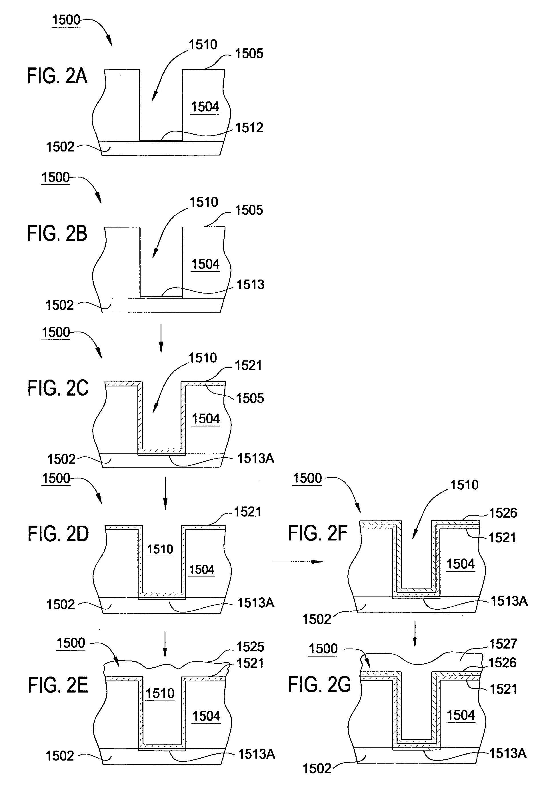
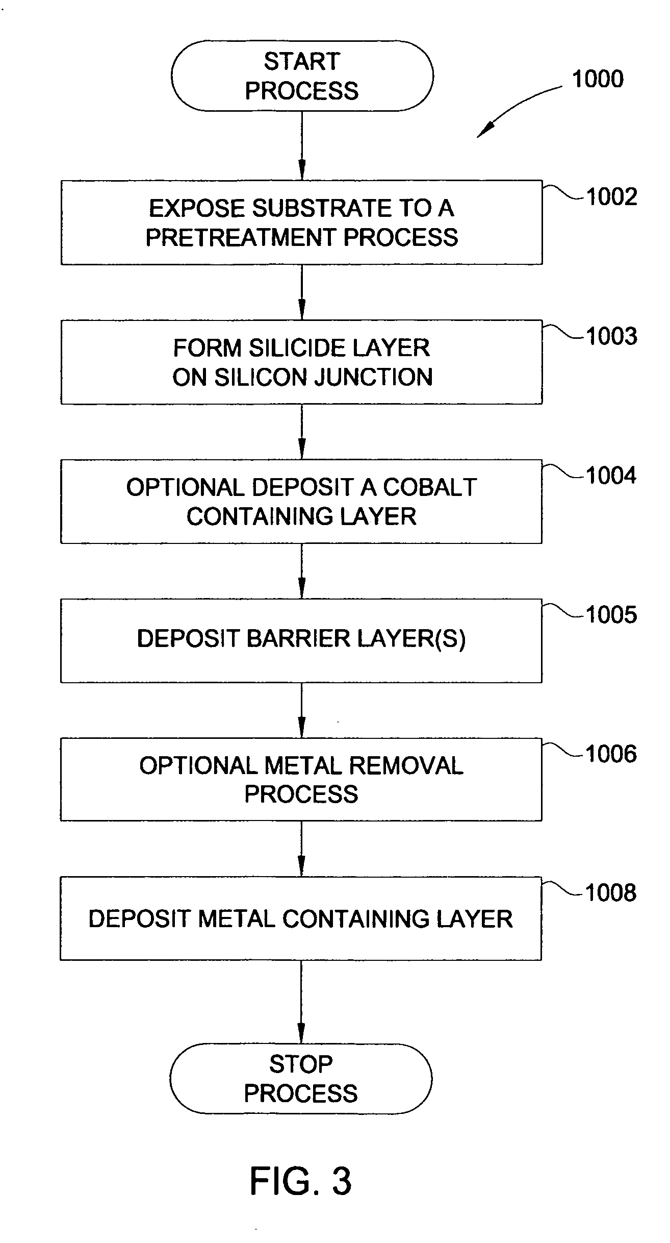
[0025] Embodiments of the invention generally provide methods of filling contact level features formed in a semiconductor device by depositing a barrier layer over the contact feature and then filing the layer using an PVD, CVD, ALD, electrochemical plating process (ECP) and / or electroless deposition processes. The term “barrier layer” as used herein is generally intended describe a single layer, or two or more layers, that act as an adhesion layer and a diffusion barrier for the subsequently deposited metal layer(s). In one embodiment, the barrier layer has a catalytically active surface that will allow the electroless deposition of a metal on the barrier layer. In one aspect, the electrolessly deposited metal is copper or a copper alloy. Copper alloys may be useful to improve the device speed and performance, help prevent electromigration or stress migration degradation during subsequent processing, improve the manufacturing device yield and device lifetime due to electromigration...


PUM

PropertyMeasurementUnit
thicknessaaaaaaaaaa
thicknessaaaaaaaaaa
thicknessaaaaaaaaaa

Abstract

Embodiments of the invention generally provide methods of filling contact level features formed in a semiconductor device by depositing a barrier layer over the contact feature and then filing the layer using an PVD, CVD, ALD, electrochemical plating process (ECP) and/or electroless deposition processes. In one embodiment, the barrier layer has a catalytically active surface that will allow the electroless deposition of a metal on the barrier layer. In one aspect, the electrolessly deposited metal is copper or a copper alloy. In one aspect, the contact level feature is filled with a copper alloy by use of an electroless deposition process. In another aspect, a copper alloy is used to from a thin conductive copper layer that is used to subsequently fill features with a copper containing material by use of an ECP, PVD, CVD, and/or ALD deposition process. In one embodiment, a portion of the barrier layer is purposely allowed to react with traces of residual oxide at the silicon junction of the contact level feature to form a low resistance connection.

Description

CROSS-REFERENCE TO RELATED APPLICATIONS [0001] This application claims benefit of U.S. Provisional Patent Application Ser. No. 60 / 663,493, filed Mar. 18, 2005 [APPM 9916L], U.S. Provisional Patent Application Ser. No. 60 / 683,599, filed May 23, 2005 [APPM 9916L02], U.S. Provisional Patent Application Ser. No. 60 / 703,538, filed Jul. 29, 2005 [APPM 9916L03], U.S. Provisional Patent Application Ser. No. 60 / 703,633, filed Jul. 29, 2005 [APPM 9916L04], U.S. Provisional Patent Application Ser. No. 60 / 709,564, filed Aug. 19, 2005 [APPM 9916L05], and U.S. Provisional Patent Application Ser. No. 60 / 754,230, filed Dec. 27, 2005 [APPM 9916L06], which are all herein incorporated by reference.BACKGROUND OF THE INVENTION [0002] 1. Field of the Invention [0003] Embodiments of the invention generally relate to methods for depositing materials on a substrate, and more specifically to methods for filling apertures within a contact formed on a substrate. [0004] 2. Description of the Related Art [0005] ...

Claims


Application Information

Patent Timeline
Patent Type & Authority Applications(United States)
IPC IPC(8): B05D5/12
CPCB82Y30/00H01L23/53238C23C16/0281C23C16/045C23C16/14C23C18/1608C23C18/1651C23C18/1653C23C18/1678C23C18/31C23C18/32C23C18/34C23C18/38C23C18/40C23C18/48C25D5/34H01L21/02063H01L21/02074H01L21/28518H01L21/28556H01L21/288H01L21/2885H01L21/76814H01L21/76843H01L21/76844H01L21/76846H01L21/76847H01L21/76849H01L21/76855H01L21/76856H01L21/76861H01L21/76862H01L21/76874H01L21/76877H01L21/76879C23C16/0227H01L2924/0002H01L2924/00
Inventor WEIDMAN, TIMOTHY W.WIJEKOON, KAPILA P.ZHU, ZHIZEKHANDELWAL, AMITSHANMUGASUNDRAM, ARULKUMARYANG, MICHAEL X.MEI, FANGMOGHADAM, FARHAD K.
Owner APPLIED MATERIALS INC
Why Eureka
Try Eureka