Low temperature method for minimizing copper hillock defects

a technology of low temperature and defect, applied in the direction of semiconductor/solid-state device manufacturing, basic electric elements, electric apparatus, etc., can solve the problems of low rc interconnect delay, more difficult processing, and remained reliability problems, so as to prevent the formation of surface discontinuities

Inactive Publication Date: 2006-11-09
TAIWAN SEMICON MFG CO LTD
View PDF19 Cites 16 Cited by
  • Summary
  • Abstract
  • Description
  • Claims
  • Application Information

AI Technical Summary

Benefits of technology

[0012] A method is also disclosed comprising the steps of: (a) depositing a copper layer on a substrate; (b) planarizing the copper layer; (c) annealing the copper layer while exposing the copper layer to a reductive gas environment comprising hydrogen; and (d) applying a dielectric layer over the copper layer using CVD; wherein the annealing step substantially removes copper oxides from the surface of the copper layer, thereby preventing formation of surface discontinuities in the copper layer during the step of applying the dielectric layer.

Problems solved by technology

Copper is a lower resistivity metal than aluminum, which results in lower RC interconnect delay.
Copper has also been shown to have superior electromigration characteristics over aluminum, but is more difficult to process, primarily because it is more difficult to etch, and it acts as a deep level trap in silicon (Si) based devices.
Although copper has desirable functional properties that make its use advantageous for forming interconnect and via structures, some reliability issues remain.
For example, copper interconnects can suffer from the problem of hillock formation due to stresses resulting from the various high temperature process steps required to form semiconductor devices.
If the hillocks are sufficiently large, they can protrude through any overlying dielectric or other layers and cause short circuiting between metal layers.
Since the oxide formation process is uncontrolled, the oxide layer is typically uneven, and as such it can cause unbalanced expansion of Cu grains when the structure is subjected to high temperatures (e.g. during subsequent CVD).
The resulting difference in expansion rates across the uneven copper oxide layer can induces hillocks.
As a result, compressive stresses build in the metal film.
As noted, these protruding hillocks can adversely affect the ability of overlying dielectric layers to adequately passivate the top surface of the underlying copper structure.
If hillocks are large enough, they can protrude through the dielectric layer and result in short-circuit types of defects either immediately or over time, which irrevocably damage the integrated circuit.

Method used


Image

  • Low temperature method for minimizing copper hillock defects
  • Low temperature method for minimizing copper hillock defects
  • Low temperature method for minimizing copper hillock defects

Examples


Embodiment Construction

[0020] According to an embodiment of the present invention, disclosed herein is a low temperature process for inhibiting the formation of hillocks in copper semiconductor structures when the structures are exposed to the temperatures involved in semiconductor processing.

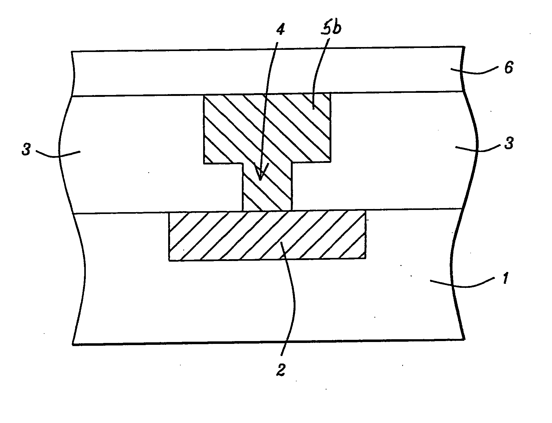
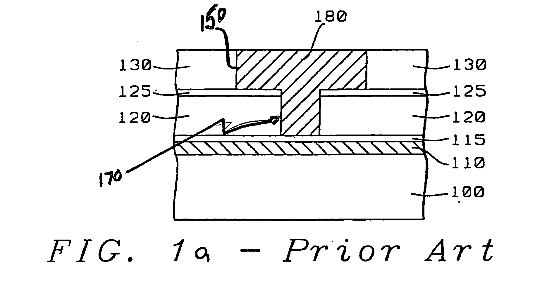
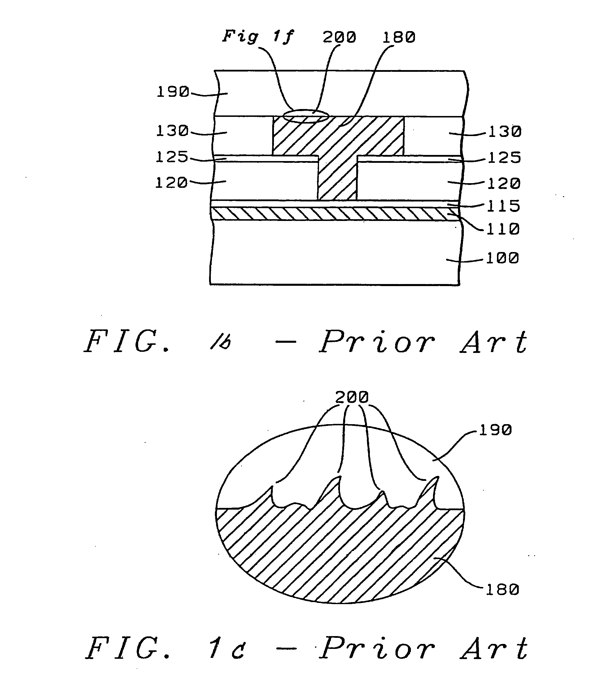
[0021] As shown in FIG. 2, a substrate 1 is provided with a conductive layer 2, and an upper insulating layer 3. Substrate 1 can be any appropriate semiconductor subtrate such as monocrystalline silicon, or alternatively it could be an insulator such as silicon dioxide, borosilicate glass (BSG), borophosphosilicate glass (BPSG) or the like. Conductive layer 2 can be copper, aluminum or tungsten, while upper insulating layer 3 can be any suitable passivation material as are known in the art, such as silicon dioxide, BSG, BPSG, etc.. Upper insulating layer 3 can be deposited using a technique such as CVD.

[0022] An opening 4 is then formed in the upper insulating layer 3 using, for example, a dual damascene technique ...


PUM

PropertyMeasurementUnit
temperatureaaaaaaaaaa

Abstract

A method of fabricating a copper interconnect on a substrate is disclosed in which the interconnect and substrate are subjected to a low temperature anneal subsequent to polarization of the interconnect and prior to deposition of an overlying dielectric layer. The low temperature anneal inhibits the formation of hillocks in the copper material during subsequent high temperature deposition of the dielectric layer. Hillocks can protrude through passivation layer, thus causing shorts within the connections of the semiconductor devices formed on the substrate. In one example, the interconnect and substrate are annealed at a temperature of about 200 ° C. for a period of about 180 seconds in a forming gas environment comprising hydrogen (5 parts per hundred) and nitrogen (95 parts per hundred).

Description

FIELD OF THE INVENTION [0001] The present invention relates to a method for fabricating integrated circuit devices. BACKGROUND OF THE INVENTION [0002] Copper is preferred in forming metal interconnects in ultra-large scale integrated ULSI semiconductor devices. This is because, as semiconductor device geometries continue to scale down below 0.25 μm, and approach 0.13 μm feature sizes, the metal interconnect lines which carry current between devices on a chip begin to dominate the overall circuit speed. In order to enhance interconnect speed and reliability, the semiconductor industry is moving away from blanket deposition and etch of aluminum (Al) based metallization towards single-damascene and dual-damascene interconnect structures with copper (Cu) based metallizations. [0003] Copper is a lower resistivity metal than aluminum, which results in lower RC interconnect delay. Copper has also been shown to have superior electromigration characteristics over aluminum, but is more diffic...

Claims


Application Information

Patent Timeline
Patent Type & Authority Applications(United States)
IPC IPC(8): H01L21/4763H01L21/44
CPCH01L21/76801H01L21/76883H01L21/76877
Inventor WU, JUNLEE, WEN-LONGNI, CHYI-TSONGLIN, SHIH-CHI
Owner TAIWAN SEMICON MFG CO LTD
Why Eureka
Try Eureka