

Magnetic thin film or composite magnetic thin film for high frequency and magnetic device Including the same
- Summary
- Abstract
- Description
- Claims
- Application Information
AI Technical Summary
Benefits of technology
Problems solved by technology
Method used
Image

Examples
example)
(Example)
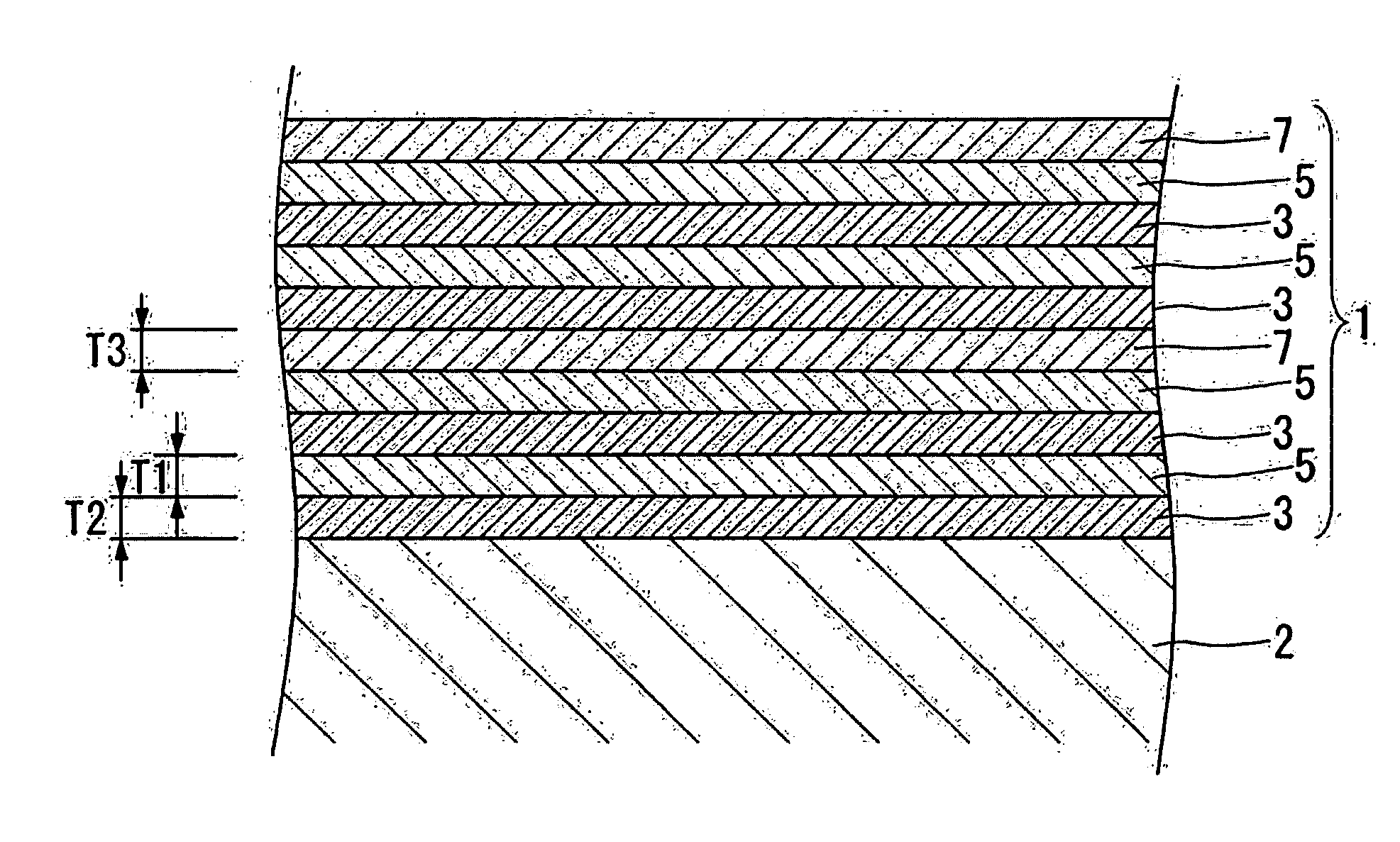
First Cycle (n=2)
[0095] The two Co based amorphous alloy layers 3 and the two T-L composition layers 5 are alternately laminated, and then the one high resistance layer 7 is laminated.
Second Cycle (n=3)
[0096] The three Co based amorphous alloy layers 3 and the three T-L composition layers 5 are alternately laminated, and then the one high resistance layer 7 is laminated.
[0097] Here, the Co based amorphous alloy layer 3 is denoted by (3), the T-L composition layer 5 is denoted by (5), and the high resistance layer 7 is denoted by (7); the laminating configuration in which the first cycle (n=2) and the second cycle (n=3) are alternately repeated twice is shown below: (3)(5)(3)(5)(7)(3)(5)(3)(5)(3)(5)(7)(3)(5)(3)(5)(7)(3)(5) (3)(5)(3)(5)(7)
[0098] Next, description will be made below on a substrate 2 on which the magnetic thin film for high frequency 1 of the present invention is formed.
[0099] Examples of the substrate 2 (FIG. 1) on which the magnetic thin film for high...
example 1
[0116] The magnetic thin film for high frequency of the present invention was prepared on the basis of the following deposition method.
(Deposition Procedure)
[0117] A Si wafer with a 100 nm thick SiO2 deposited thereon was used as the substrate.
[0118] By use of a multi-target simultaneous sputtering apparatus, a magnetic thin film for high frequency was deposited on the substrate in a manner to be described later. More specifically, the interior of the multi-target simultaneous sputtering apparatus was preliminarily evacuated down to 8×10⁻⁵ Pa, thereafter Ar gas was introduced until the pressure of the interior reached 10 Pa, and the surface of the substrate was subjected to sputtering etching at an RF power of 100 W for 10 minutes.
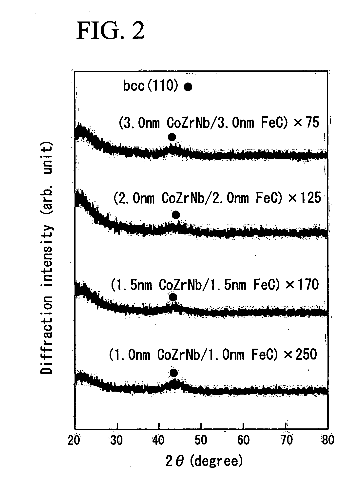
[0119] Subsequently, the Ar gas flow rate was adjusted so as for the pressure to be 0.4 Pa, at a power of 300 W, a CO87Zr5Nb8 target, a composite target composed of a Fe target and C (carbon) pellets arranged thereon and a composite target composed of...
example 2
(Deposition Cycle)
[0125] There was repeated three times a deposition cycle in which a 1.5 nm thick CoZrNb layer was deposited as a first layer on the substrate, and thereafter a 1.5 nm thick Fe—C layer was deposited thereon as a second layer. Successively, a 1.0 nm thick FeCoAlO layer was deposited on the sixth layer. There was repeated by 50 cycles a deposition treatment cycle in which, as described above, the three CoZrNb layers and the three Fe—C layers were alternately laminated and thereafter the one FeCoAlO layer was laminated, and thus there was obtained a composite magnetic thin film (Example 2) having a magnetic thin film configuration shown in FIG. 12 (the total thickness: 500 nm). The deposition procedures were the same as in Example 1 described above.
Example 3
(Deposition Cycle)
[0126] A 20.0 nm thick CoZrNb layer was deposited as a first layer on the substrate, and thereafter a 5.0 nm thick Fe—C layer was deposited thereon as a second layer. Successively, a 2.0 nm t...
PUM
| Property | Measurement | Unit |
|---|---|---|
| Thickness | aaaaa | aaaaa |
| Magnetic field | aaaaa | aaaaa |
| Magnetic field | aaaaa | aaaaa |
Abstract
Description
Claims
Application Information