Method of forming a trench structure having one or more diodes embedded therein adjacent a PN junction

a trench structure and diode technology, applied in the direction of diodes, semiconductor devices, electrical equipment, etc., can solve the problems of high power loss, primarily power loss, and high density, and achieve the effect of increasing the blocking voltage of the semiconductor structur

Inactive Publication Date: 2006-11-16
SEMICON COMPONENTS IND LLC
View PDF99 Cites 15 Cited by
  • Summary
  • Abstract
  • Description
  • Claims
  • Application Information

AI Technical Summary

Benefits of technology

[0011] In another embodiment, a body region is formed in the epitaxial layer. The body region is one of the P-type and N-type regions and the other one of the P-type and N-type regions forms a drift region. The diode is arranged in the first trench such that when the semiconductor structure is biased in a blocking state an electric field induced in the at least one diode influences an electric field in the drift region to thereby increase the blocking voltage of the semiconductor structure.

Problems solved by technology

However, the higher density does not necessarily improve power loss in mid to high voltage range (e.g., 60 to 2000 volts) devices.
In such devices, the power loss is primarily due to the high resistivity of the drift region (e.g., region 106 in FIG. 1).
The high resistivity of the drift region results in a higher on-resistance, which in turn results in high power loss.
Since a high blocking voltage is a critical feature for mid to high voltage power devices, increasing the drift region doping is not an option.
Similar issues are present in power diode devices.
When the base and source regions are annealed during a thermal cycle, the dopants in the opposite polarity regions undesirably diffuse into each other.
This dopant inter-diffusion makes the thermal processing difficult and limits shrinking of the cell pitch.
The inability to shrink the cell pitch is especially problematic in mid to low voltage devices in which the power loss occurs primarily in the channel region rather than in the drift region.
The columnar opposite polarity regions technique is thus unattractive for mid to low voltage devices as it can not be shrunk.

Method used


Image

  • Method of forming a trench structure having one or more diodes embedded therein adjacent a PN junction
  • Method of forming a trench structure having one or more diodes embedded therein adjacent a PN junction
  • Method of forming a trench structure having one or more diodes embedded therein adjacent a PN junction

Examples


Embodiment Construction

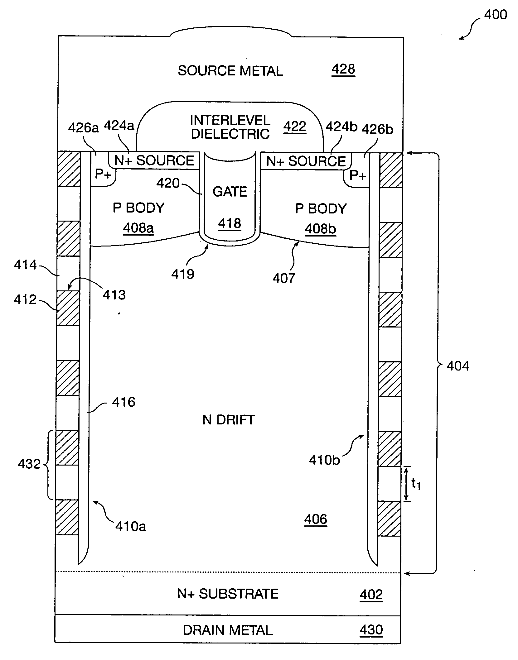
[0020] Embodiments of a trench having one or more diodes embedded therein and methods of forming the same are described in accordance with the invention. The diode trench structure can be used in semiconductor devices required to withstand high voltages. The diode trench helps achieve high current capability, high breakdown voltage, low forward voltage drop, and a small cell pitch.

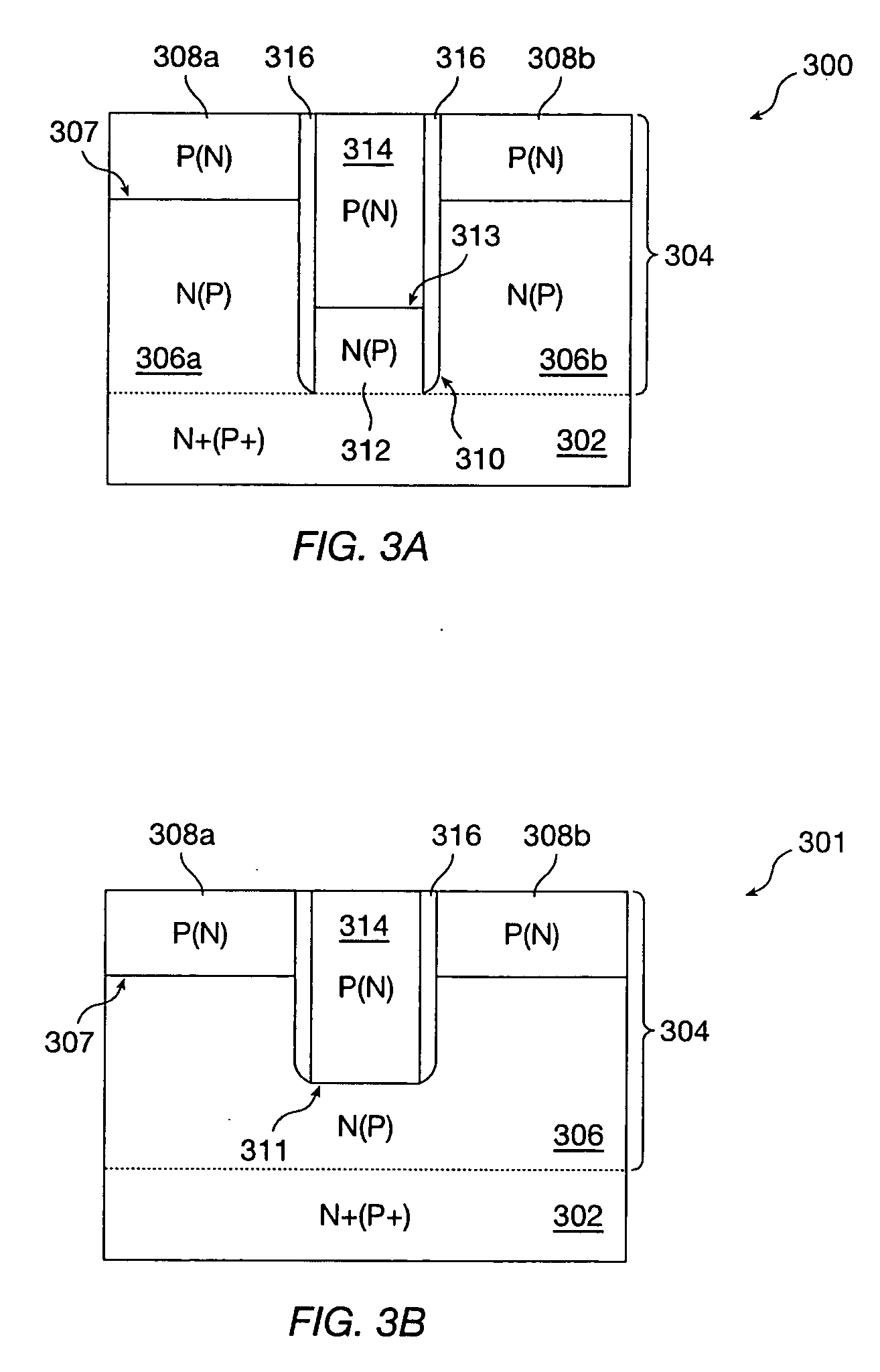
[0021]FIG. 3A shows a cross-section view of a semiconductor structure 300 having a trench 310 in accordance with one embodiment of the present invention. An epitaxial layer 304 is formed over and is of the same conductivity type as a substrate 302. Regions 308a,b of opposite conductivity type to epitaxial layer 304 is formed along a top portion of epitaxial layer 304. Trench 310 extends from a top surface of epitaxial layer 304 through to substrate 310. Trench 310 may alternatively be terminated at a shallower depth (i.e., within regions 306a,b of epitaxial layer 304.) Trench 310 includes a diode made up ...


PUM


Abstract

A semiconductor structure is formed as follows. A semiconductor region is formed to have a P-type region and a N-type region forming a PN junction therebetween. A first trench is formed extending in the semiconductor region adjacent at least one of the P-type and N-type regions is formed. At least one diode is formed in the trench.

Description

CROSS-REFERENCES TO RELATED APPLICATIONS [0001] This application is a division of U.S. application Ser. No. 10 / 288,982, filed Nov. 5, 2002, which is incorporated by reference in its entirety for all purposes.BACKGROUND OF THE INVENTION [0002] The present invention relates in general to semiconductor technology and in particular to high-voltage semiconductor structures and methods of manufacturing the same. [0003]FIG. 1 shows a cross-section view of a portion of a conventional power MOSFET having a buried-gate structure. A highly-doped substrate 102 forms the drain contact for MOSFET 100. An epitaxial layer 104 formed over substrate 102 includes source regions 124a,b formed in body regions 108a,b. Body regions 108a,b are flanked on one side by gate trench 119. P+ regions 126a,b form the areas through which contact is made to body regions 108a,b. Gate trench 119 is filled with polysilicon forming the MOSFET gate 118. When MOSFET 100 is turned on, current travels in a vertical directio...

Claims


Application Information

Patent Timeline
Patent Type & Authority Applications(United States)
IPC IPC(8): H01L21/8234H01L29/06H01L29/40H01L29/78H01L29/861
CPCH01L29/0653H01L29/404H01L29/407H01L29/861H01L29/7802H01L29/7813H01L29/7801H01L29/7816H01L29/7818
Inventor KOCON, CHRISTOPHER BOGUSLAWYEDINAK, JOSEPH ANDREW
Owner SEMICON COMPONENTS IND LLC
Why Eureka
Try Eureka