
Process for producing improved membranes

a technology of membranes and processing methods, applied in the direction of grinding machines, electrical equipment, basic electric elements, etc., can solve the problems of non-planar outer surface, non-planar further layers placed on the outer layer, and general thinness of silicon wafers that are subjected to the process, so as to improve the performance characteristics of the membranes and improve the performance of the carrier head

Inactive Publication Date: 2006-11-16
SYST ON SILICON MFG PTE
View PDF8 Cites 3 Cited by
  • Summary
  • Abstract
  • Description
  • Claims
  • Application Information

AI Technical Summary

Benefits of technology

[0014] The applicants of the present application were able to ascertain that significantly improved membrane performance in carrier heads could be achieved by treating the membranes either during membrane manufacture or as a step prior to using the membrane. In particular the applicants found that subjecting the current membranes to elevated temperatures improved the performance characteristics of the membranes.
[0015] The applicants have been successful in identifying process conditions that may be applied to existing membranes so that they have improved performance relative to untreated membranes. This allows existing membranes that can be purchased commercially to be converted into membranes with improved performance.
[0016] In one aspect the present invention provides a method of improving the performance of a flexible membrane for use in a chemical mechanical polishing system, the method including subjecting the flexible membrane to elevated temperatures.
[0022] It has been found that by using membranes that have been subjected to a process of this type membrane failure during the chemical / mechanical polishing of wafers is significantly lowered. This in turn leads to significantly reduced machine downtime as the heads have to be rebuilt far less frequently and the number of dropped wafers is also significantly reduced. This therefore leads to considerably higher manufacturing efficiency.
[0023] As stated previously the membranes that have been subjected to the process may be used in any carrier head for chemical / mechanical polishing that includes a flexible membrane. When the membranes treated by the process are utilised in carrier heads of this type the carrier heads typically demonstrate improved performance due to lower levels of membrane failure.

Problems solved by technology

One problem that potentially occurs in this process is that as the sequential layers are deposited and etched in this way, the outer surface becomes increasingly non-planar.
This in turn causes difficulty as if the outer surface is non-planar then, as a consequence, any further layers placed on the outer layer will also be non-planar.
A problem identified in the development of the carrier heads of this type has been the need to design a head that does not damage sensitive substrates such as the silicon wafers during handling.
Silicon wafers that are subjected to the process are generally very thin and hence are not ideally suited to being brought into contact with any hard surfaces during movement operations.
In addition, even if the surface of the head can be padded in some way there is the risk that the point of contact with the wafer may cause the surface of the wafer to become marked.
One problem typically encountered with the use of a flexible membranes in carrier heads of these types is membrane failure whilst in use.
The failure of the membrane cannot be accurately predicted by conventional test procedures which do not damage the membrane.
Accordingly it is not possible to test individual membranes prior to use and as such membrane failure typically occurs when in use.
With existing membranes the failure rate is approximately 3.5 failures per 10,000 wafer moves.
This leads to significant downtime consequences as membrane failure typically leads to the wafer being dropped in the chemical / mechanical polishing apparatus.
Due to the high cleanliness required there is also the risk that there may be contamination of the apparatus by any broken pieces of wafer that have occurred due to wafer damage upon falling.
As will be appreciated, this leads to significant machine downtime and reduction in the overall sufficiency of the manufacturing process.
It was found that the poor membrane performance typically occurred due to poor selection of physical properties of the membranes used in that the membranes used did not have physical properties that were compatible with the conditions they were required to operate under.
Accordingly, there was an unacceptably high rate of failure of the existing membranes during use.
Without wishing to be bound by theory it is felt that insufficient membrane performance is observed when one or more of the membrane's physical properties is not within the required bounds.
Unfortunately, the ability to test these physical parameters relies on destructive means and, as such, it is not possible to accurately predict the performance of an individual membrane prior to use by testing its physical parameters.

Method used

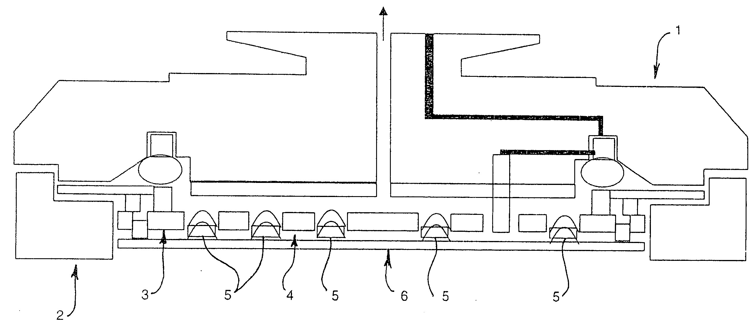
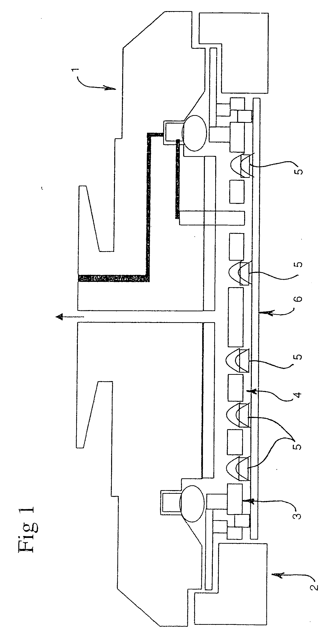
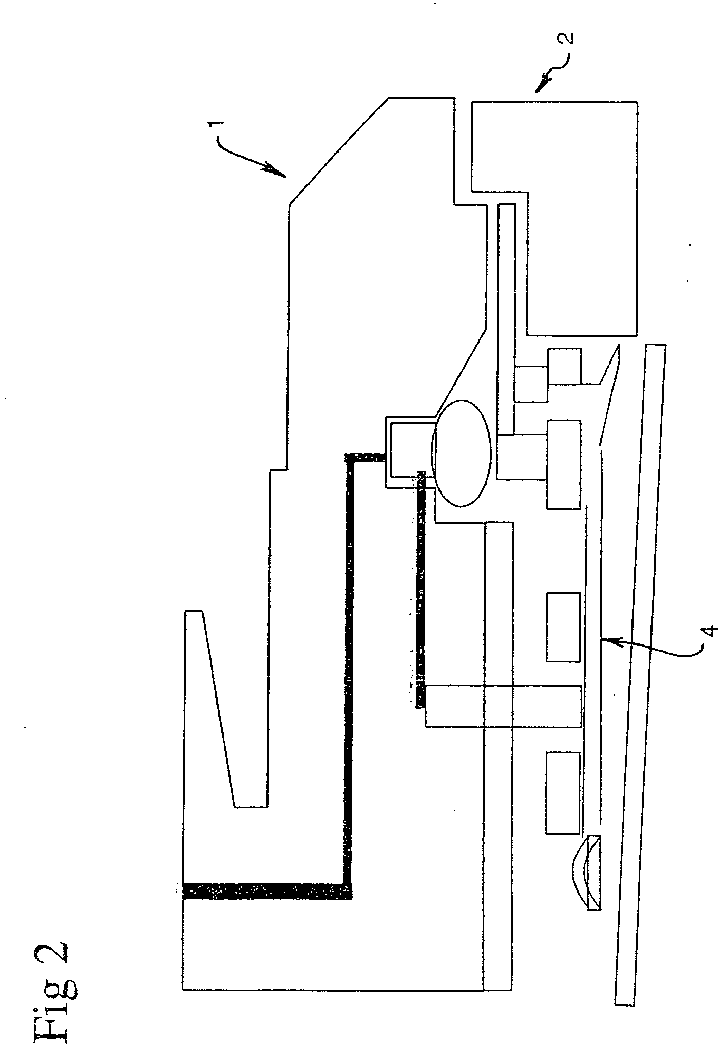

Image

  • Process for producing improved membranes
  • Process for producing improved membranes
  • Process for producing improved membranes

Examples


example 1

[0069] In order to demonstrate the process of the invention a number of silicone membranes were subjected to the process of the invention. The silicone membranes were sourced from Applied Materials under Part Number 0021-77650. A group of 18 silicone membranes were subjected to varying temperature / time regimes and a number of physical properties were then measured. The regimes were: [0070] 1. Control—no treatment. [0071] 2. 50° C. for 60 minutes. [0072] 3. 70° C. for 60 minutes. [0073] 4. 80° C. for 60 minutes. [0074] 5. 90° C. for 60 minutes.

[0075] In each case the silicone membrane was removed from the packaging, wiped with a solution of 5% IPA in water to remove surface organic compounds. The surface was then wiped with de-ionized water to clean off any remaining surface residue. The membrane is then dried and heated at the required temperature for 60 minutes. At the end of the treatment the membrane is removed from the heat source and left to cool in a clean room environment (C...

example 2

[0078] A number of silicon membranes were prepared according to the general method outlined in Example 1. These were then subjected to a wafer grip test.

[0079] This typically involves placing a membrane on the carrier head and inverting it on a test surface. A transport cover is slid over the head and the wafer grip test function is activated. The retaining ring is then pressurized and presses against the cover. This is followed by the membrane being pushed against the cover by pressure until it presses flat on the cover to make full contact. The membrane is then subjected to vacuum which creates small suction cups with the help of a perforated backing plate which grips the cover. In order to rate a pass the membrane must stick to the cover for at least 1 minute. If the membrane fails it collapses immediately when the vacuum is applied.

[0080] For each membrane the grip test was performed 10 times. The applicants have found that the results of the grip test correlate to membrane pe...

example 3

[0082] As a result of the improvements demonstrated by the membranes treated by the process of the invention it was decided to take a batch membranes that had been subjected to the process of the invention. These were then trialled in a pilot scale laboratory under full factory operating condition. This was to enable to full number of wafer movements to be carried out to ensure that the date obtained was statistically significant. The results are shown as FIG. 3. As can be seen in FIG. 3 the prior art membrane had a rate of membrane failure such that there were 3.35 wafer slips per 10,000 membrane movements. Following replacement of the prior art membrane with membranes that had been treated thus reduced to 1.47 wafer slips per 10,000 movements. This demonstrates the efficacy of the process of the invention in improving flexible membrane performance.


PUM

PropertyMeasurementUnit
temperatureaaaaaaaaaa

Abstract

The present invention relates generally to the field of chemical / mechanical polishing of substrates. In particular the invention relates to methods of producing improved membranes for use in chemical / mechanical polishing systems. The present invention provides a method of improving the properties of a flexible membrane for use in chemical / mechanical polishing, the method including subjecting the membrane to elevated temperatures.

Description

FIELD OF THE INVENTION [0001] The present invention relates generally to the field of chemical / mechanical polishing of substrates. In particular the invention relates to methods of producing improved membranes for use in chemical / mechanical polishing systems. BACKGROUND OF THE INVENTION [0002] With the rapid development of the electronics industry in recent years there has been phenomenal growth in the need for integrated circuits. As such there has been a significant focus world-wide on improving methods of manufacture of integrated circuits with a view to increasing production speed / efficiency. In general integrated circuits may be formed on a number of materials but they are typically formed on silicon wafers. The process of manufacture of integrated circuits of this type typically involves the sequential deposition of a number of layers of conductive, semi-conductive or insulating layers onto the outer surface of a wafer. Using the process a number of layers are built up sequent...

Claims


Application Information

Patent Timeline
Patent Type & Authority Applications(United States)
IPC IPC(8): B24B29/00B24B37/30B24D3/22H01L21/304
CPCB24B37/30
Inventor KOH, MENG FEIPOH, CHOON SIONGGOH, INN SWEELEONG, THENG WEINEO, TECK LEONGWANG, BING
Owner SYST ON SILICON MFG PTE
Learn More