Superconducting film and method of manufacturing the same

a technology of superconducting film and manufacturing method, which is applied in the direction of superconductor devices, vacuum evaporation coating, transportation and packaging, etc., can solve the problems of difficult to control the density per unit area of dislocation, difficulty in controlling the inclination of boundary planes, artificial defects, etc., and achieves excellent pinning efficiency, low cost, and high jc.

Inactive Publication Date: 2006-11-16
JAPAN SCI & TECH CORP +1
View PDF7 Cites 26 Cited by
  • Summary
  • Abstract
  • Description
  • Claims
  • Application Information

AI Technical Summary

Benefits of technology

[0008] An object of the present invention is to provide a structure of ideal pinning centers in a superconducting film which is formed on a substrate and a method of introducing the pinning centers. Another object of the invention is to provide, at low cost, a technique for increasing Jc which can be applied to all Type II superconductors of film shape.
[0015] According to the present invention configured as described above, strong pinning centers having excellent pinning efficiency can be introduced into a superconducting film, and a superconducting film having very high Jc can be manufactured at low cost. Since the pinning centers introduced into a superconducting film of the invention are aligned in a current flowing direction, these pinning centers will not impede a current flowing path. Therefore, a superconducting film of the invention is useful in applications which require flowing large currents, such as cables, magnets, shields, current limiters, microwave devices, and semifinished products of these articles.

Problems solved by technology

According to the report, dislocation densities of 10 μm−2 to 100 μm−2 can be obtained by changing film forming conditions in various ways and Jc increases with increasing dislocation density, although it is difficult to control the density per unit area of dislocations which are naturally introduced during film growth.
In general, however, boundary planes exist randomly, it is difficult to control Jc by controlling the inclination of boundary planes.
Furthermore, artificial defects introduced by lithography and columnar crystal defects introduced by electron beam irradiation and heavy ion irradiation also become pinning centers.
Although this method is effective in artificial pin introduction, from a practical viewpoint, the throughput is low and the cost is too high for a large area fabrication and for wire fabrication.
However, the equipment cost and the cost of ion acceleration are very high.
Furthermore, in some cases materials are radioactivated and hence these methods are not practical.
Therefore, these techniques have their limits in drastically improving Jc.

Method used


Image

  • Superconducting film and method of manufacturing the same
  • Superconducting film and method of manufacturing the same
  • Superconducting film and method of manufacturing the same

Examples


example 1

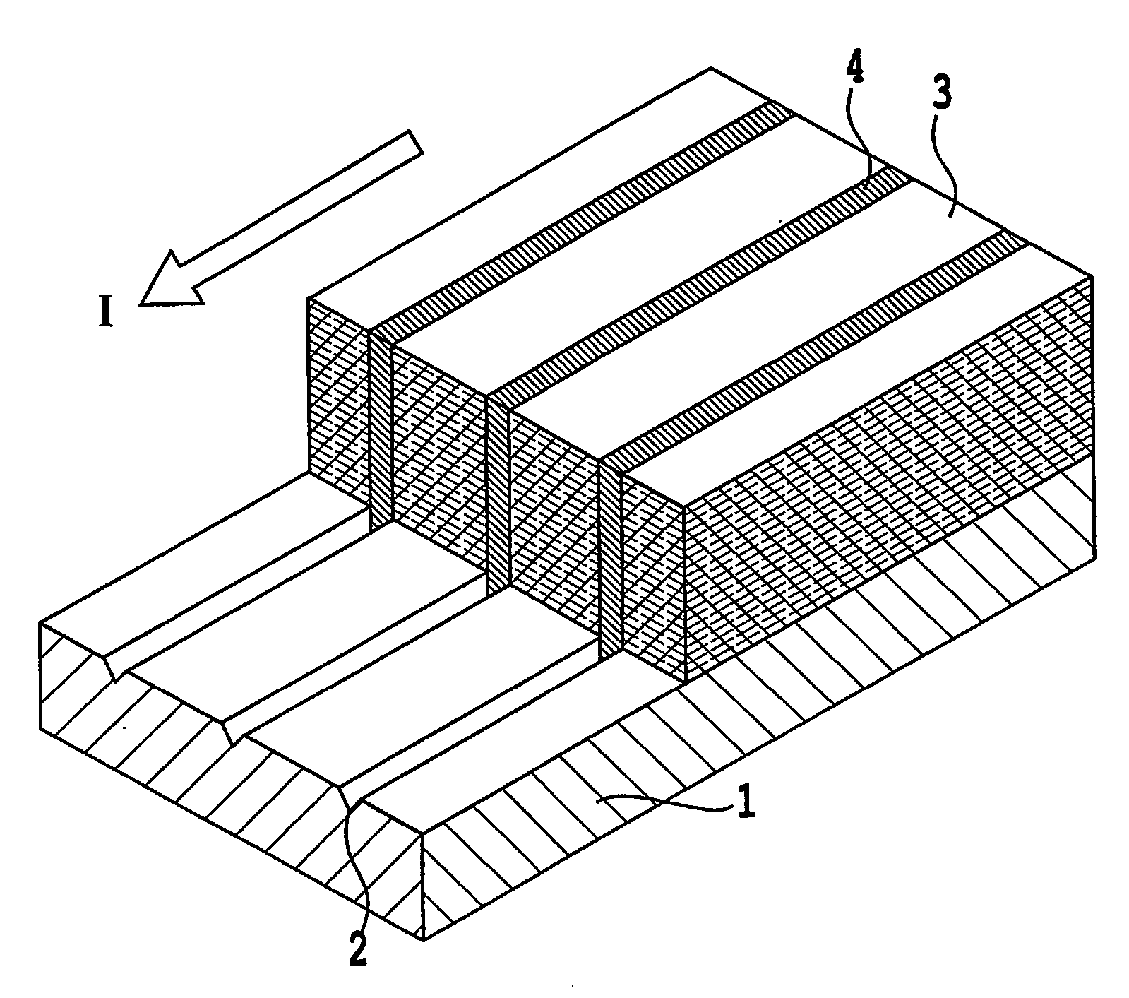
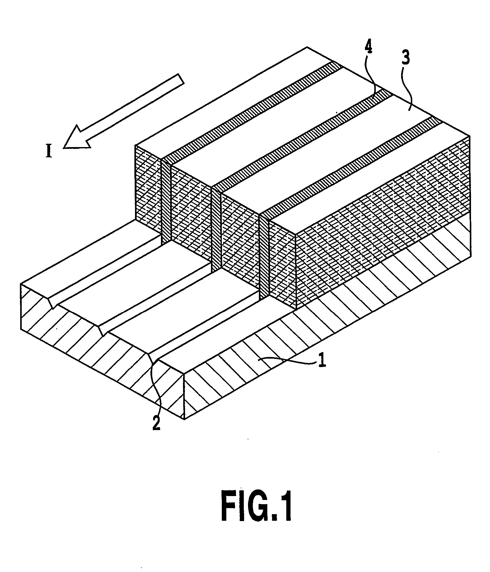
[0062] First, nano grooves were formed on a single-crystal substrate. An SrTiO3 substrate 3 mm wide×10 mm long×0.5 mm thick, the (100) plane of which was mirror-like polished, was prepared as the single-crystal substrate. Subsequently, nano grooves were formed in a region of 60 μm×60 μm in the central part of this substrate surface by utilizing AFM in processing mode. With the width and depth of the nano grooves set at 30 nm respectively and the length of the nano grooves at 60 μm, 330 nano grooves were formed in the above-described region with equal spacing such that the nano grooves become parallel to the longitudinal direction of the substrate. The average spacing of the centers of the nano grooves was 150 nm. With the substrate fixed on a heater provided within a vacuum chamber, a thin film of YBa2Cu3O7−x (YBCO) was formed on the substrate by the excimer pulsed laser deposition (PLD) method and a superconducting film (I-1) was obtained. At this time, a flat SrTiO3 substrate 3 mm...

example 2

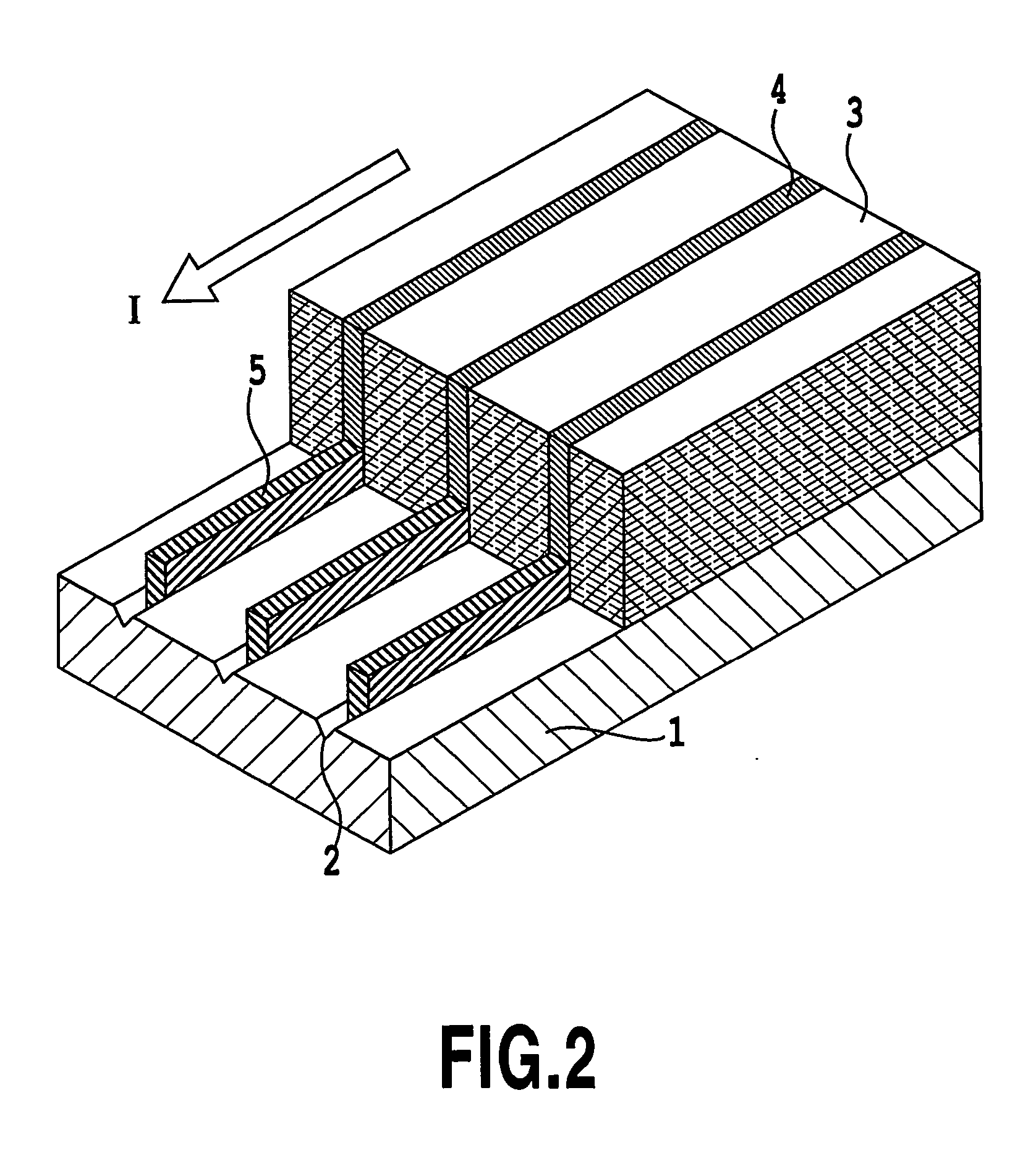
[0065] Nano grooves were formed on an SrTiO3 substrate in the same manner as in Example 1. Next, the substrate on which nano grooves had been formed was fixed on a heater within a vacuum heater for PLD, and defect inducing parts were formed on the nano grooves by the PLD method. Y2O3 was used as the material for the defect inducing parts. A Y2O3 sintered compact target was ablated using 30 pulses of an excimer laser, and Y2O3 was deposited on the SrTiO3 substrate. At this time, the substrate temperature was 700° C. and the partial oxygen pressure was 10−5 Torr (1.33×10⁻³ Pa). Under these conditions, Y2O3 deposited only on the nano grooves to form the defect inducing parts. Then, the temperature was lowered to room temperature and in the same manner as in Example 1, an SrTiO3 substrate without a nano groove was attached on the heater, beside the sample with nano grooves and defect inducing parts. Then, in the same manner as in Example 1, YBCO films were formed by the PLD method using...

example 3

[0067] First, nano holes were formed on a single-crystal substrate. An SrTiO3 substrate 3 mm wide×10 mm long×0.5 mm thick, the (100) plane of which was mirror-like polished, was prepared as the single-crystal substrate. Rows of nano holes were formed in a region of 60 μm×60 μm in the central part of this substrate surface by use of electron beam lithography. The width and depth of the nano holes were 40 nm and 20 nm, respectively. The rows of nano holes were arranged so as to be parallel to the length direction of the substrate and so that the length of the rows became 60 μm. The spacing between the nano holes in the longitudinal direction of the substrate was 100 nm, and 330 rows of nano holes were formed in the above-described region 60 μm×60 μm with equal spacing. The average spacing of the centers of the nano hole rows was 150 nm. With this substrate fixed on a heater provided within a vacuum chamber, a thin film of YBa2Cu3O7−x (YBCO) was formed on the substrate by the excimer p...


PUM

PropertyMeasurementUnit
depthaaaaaaaaaa
depthaaaaaaaaaa
diameteraaaaaaaaaa

Abstract

The present invention relates to a superconducting film having a substrate and a superconductor layer formed on the substrate, in which nano grooves are formed parallel to a current flowing direction on a substrate surface on which the superconductor layer is formed and two-dimensional crystal defects are introduced in the superconductor layer on the nano grooves, and a method of manufacturing this superconducting film. A superconducting film of the invention, which is obtained at low cost and has very high Jc, is useful in applications such as cables, magnets, shields, current limiters, microwave devices, and semifinished products of these articles.

Description

TECHNICAL FIELD [0001] The present invention relates to superconducting thin and thick films having a high critical current density in a magnetic field which can be used in the filed of cables, magnets, shields, current limiters, microwave devices, semifinished products of these articles and the like and a method of manufacturing the films. BACKGROUND ART [0002] When a magnetic field of not less than a lower critical magnetic field Hcl is applied to a superconductor, quantized flux lines (φ0=2.07×10⁻¹⁵ Wb) are formed and penetrate into the superconductor. When a current is caused to flow in this state, the Lorentz force acts on the quantized flux lines. When these quantized flux lines begin to move, a voltage is generated and the superconducting state is broken. It is known that, for example, in a superconducting film formed from a high-temperature oxide superconductor YBa2Cu3O7−x (YBCO), dot-like defects such as naturally introduced oxygen deficiency and fine impurities function as...

Claims


Application Information

Patent Timeline
Patent Type & Authority Applications(United States)
IPC IPC(8): H01L39/24C23C14/02C23C14/08H01B12/06H01B13/00
CPCC23C14/02C23C14/028C23C14/087H01L39/2454Y10T428/2457H01L39/2487Y10S505/816Y10T428/24322H01L39/2483H10N60/0576H10N60/0828H10N60/0856H01B12/06C23C14/08H10N60/01
Inventor MATSUMOTO, KANAMEMUKAIDA, MASASHIYOSHIDA, YUTAKAICHINOSE, ATARUHORII, SHIGERU
Owner JAPAN SCI & TECH CORP
Why Eureka
Try Eureka