Mask and method for electrokinetic deposition and patterning process on substrates

a technology of electrokinetic de applied in the field of masks and methods for electrokinetic deposition and patterning process on substrates, can solve the problem of limiting the application of electrokinetic deposition to substrates, and achieve the effect of facilitating electrokinetic deposition of charged particles

Active Publication Date: 2006-11-23
FRY S METALS INC
View PDF17 Cites 15 Cited by
  • Summary
  • Abstract
  • Description
  • Claims
  • Application Information

AI Technical Summary

Benefits of technology

[0010] The invention is also directed to a mask for application to a substrate to facilitate electrokinetic deposition of charged particles onto the substrate, the mask comprising an

Problems solved by technology

This requirement limits the application of electrokinetic deposi

Method used


Image

  • Mask and method for electrokinetic deposition and patterning process on substrates
  • Mask and method for electrokinetic deposition and patterning process on substrates
  • Mask and method for electrokinetic deposition and patterning process on substrates

Examples


example 1

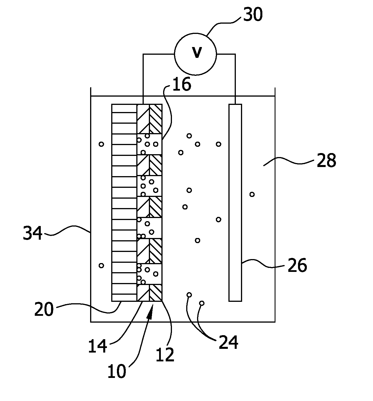
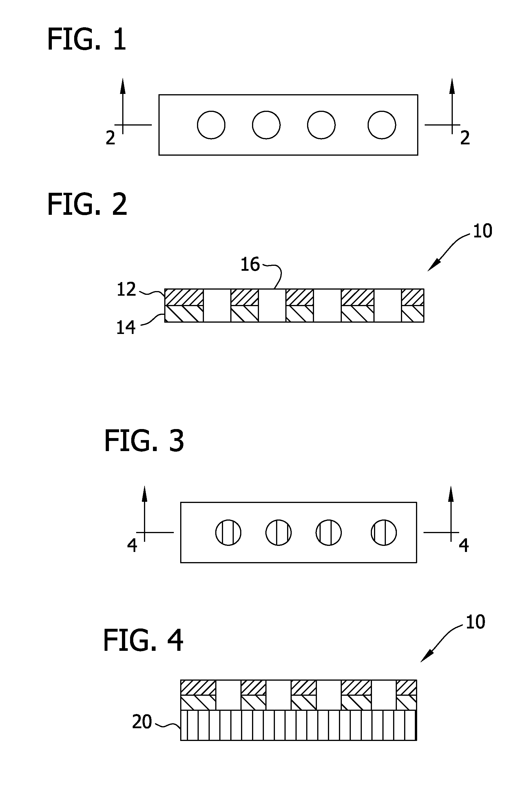
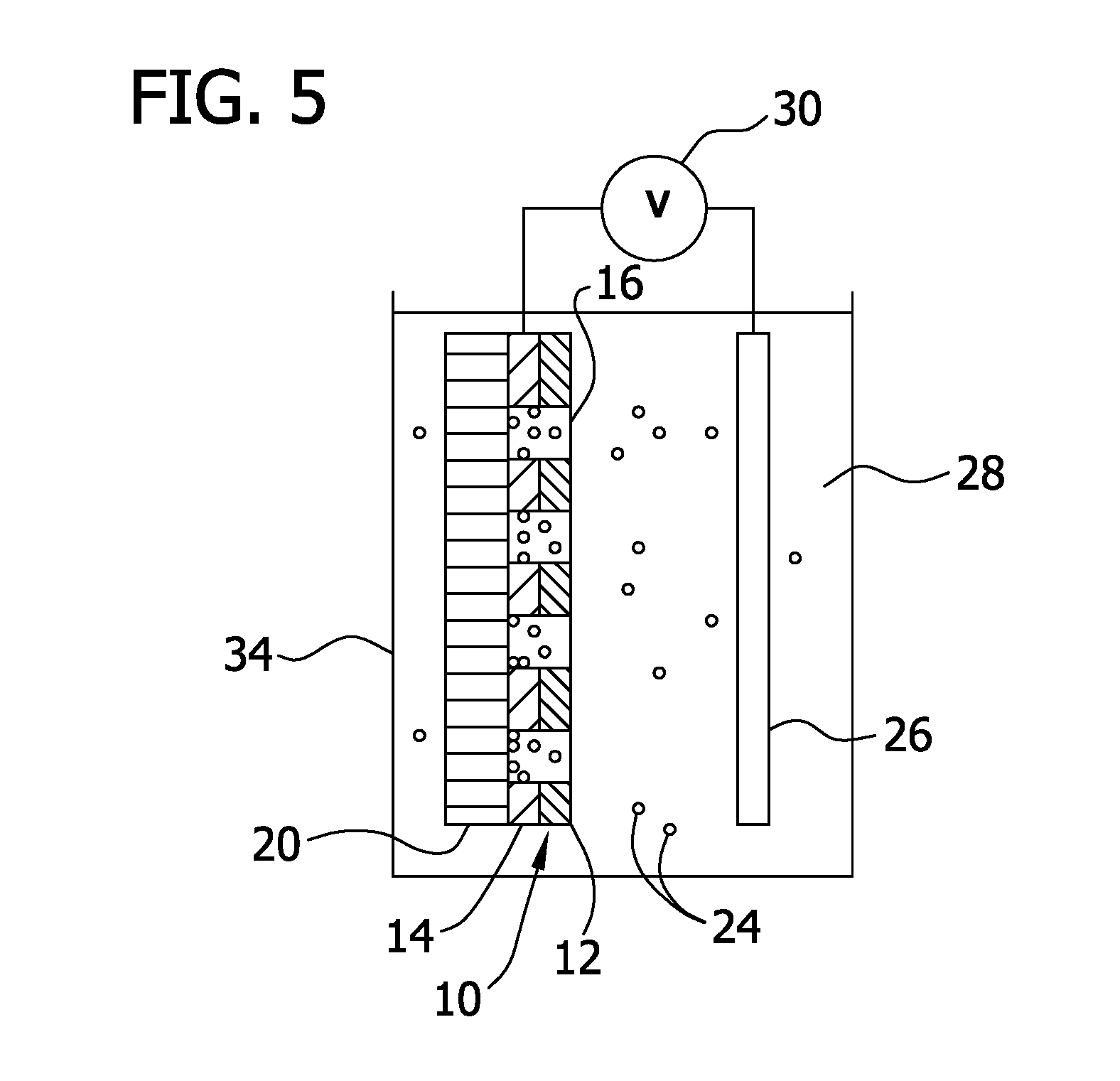
[0059] A non-conducting laminate is employed as a substrate. A mask is prepared which is a copper layer coated with solder mask, and having openings 125 μm diameter. FIGS. 6 and 7 illustrate the substrate with the mask applied thereto. The deposition is conducted in the toner similar to one described in WO 2005 / 033352, with a bath comprising Isopar, 120 g / l pretreated solder powder, and 0.5 ml of 10% barium petronate solution. The substrate with mask applied is immersed in the bath with a counter-electrode. A voltage of 200 V is applied between the copper layer and the counter-electrode. After 20 seconds, deposition openings in the mask are filled with solder powder. FIGS. 8 and 9 show the substrate after deposition of the solder powder particles.

example 2

[0060] A mask consisting of a stainless steel conductive layer with epoxy laminate was prepared by the above procedure in the pattern shown in FIG. 10. The mask was placed over a PWB substrate as shown in FIG. 11. Solder powder was deposited in the openings of the mask by the above procedure to yield solder particles on the substrate as shown in FIG. 12. This illustrates the capability of the invention for depositing at tight pitch and wide line capability.

[0061] Although the methods and materials of the invention are described above chiefly in the context of applying metal particles to substrates, the methods and materials are applicable to deposition of non-metal particles as well, provided the nature of the particles is such that they can be imparted with an electrochemical charge. Examples of such processes involving non-metal powders include deposition of phosphors, glasses, ceramics, semiconductor materials such, e.g., for use in flat panel displays or the like.


PUM

PropertyMeasurementUnit
Sizeaaaaaaaaaa
Sizeaaaaaaaaaa
Sizeaaaaaaaaaa

Abstract

A mask for application to a substrate to facilitate electrokinetic deposition of charged particles onto the substrate, the mask comprising a conducting layer, a dielectric layer, and mask openings. A method for applying a pattern of charged particles to a substrate comprising applying the foregoing the substrate to yield a masked substrate; immersing the masked substrate in a bath containing the charged particles; and establishing an electrical potential between the conducting layer of the mask and a counter-electrode thereby electrokinetically depositing the particles through the mask openings onto areas of the substrate exposed in the mask openings. Products made by this method.

Description

CROSS REFERENCE TO RELATED APPLICATION [0001] This application claims priority from provisional U.S. application 60 / 682,130, filed May 18, 2005, the entire disclosure of which is explicitly incorporated by reference.FIELD OF THE INVENTION [0002] This invention relates to a mask and method for producing patterned articles by deposition of powder, particles, spheres, or other materials onto a substrate. Applications for this technology include but are not limited to display technology (conducting and insulating traces on glass, plastics, patterning phosphorous, etc), printed electronics (solderable surfaces / solderability protectant layers, conductors, dielectrics, passive components etc), medical (patterning assay chemicals, drug dosage measures, etc), parallel assembly processes (RFID die, electronic components, etc.), and others. BACKGROUND OF THE INVENTION [0003] In a variety of applications it is desirable to apply particles to a substrate in a predetermined pattern. One such appl...

Claims


Application Information

Patent Timeline
IPC IPC(8): C25B7/00B05D1/32C25D1/12
CPCB23K3/0623H01L2924/014C25D5/022C25D13/00C25D13/22C25D15/00H01L21/2885H01L24/11H01L24/12H01L2224/11505H01L2224/13099H01L2924/01013H01L2924/01015H01L2924/01029H01L2924/01042H01L2924/01047H01L2924/01056H01L2924/01079H01L2924/01082H01L2924/04953H01L2924/09701H01L2924/3025H05K3/3484H05K2203/0425H05K2203/0557H05K2203/0776H05K2203/09H05K2203/105H01L2924/01005H01L2924/01006H01L2924/01023H01L2924/01024H01L2924/01033H01L2924/01045B23K2201/42B23K2101/42H01L2224/05001H01L2224/05023H01L2224/05124H01L2224/05155H01L2224/05171H01L2224/05568H01L2924/00014H05K3/3485H01L2224/05599H01L21/0274
Inventor KHASELEV, OSCARLEWIS, BRIAN G.MARCZI, MICHAELSINGH, BAWA
Owner FRY S METALS INC
Why Eureka
Try Eureka