Array-type modularized light-emitting diode structure and a method for packaging the structure

a light-emitting diode and array-type technology, which is applied in the direction of electrical equipment, semiconductor devices, semiconductor/solid-state device details, etc., can solve the problems of poor heat dissipation effect, affecting the light-emitting diode's light-emitting efficiency, and difficult to dissipate heat generated by the light-emitting diode from the substrate, etc., to achieve high heat conductivity, high heat conductivity, and high conductivity-

Inactive Publication Date: 2006-11-23
TSOU CHING FU +2
View PDF18 Cites 44 Cited by
  • Summary
  • Abstract
  • Description
  • Claims
  • Application Information

AI Technical Summary

Benefits of technology

[0007] It is therefore a primary object of the present invention to provide an array-type modularized light-emitting diode structure and a method for packaging the structure. The array-type modularized light-emitting diode structure includes a lower substrate and an upper substrate fixed on the lower substrate. A material with high heat conductivity is selected as the material of the upper substrate. By means of one of molding, injection molding and etching, the upper substrate being made from the material to have multiple arrayed dents and at least two through holes passing through the bottom of each dent. A material with high heat conductivity is selected as the material of the lower substrate. By means of one of halftone printing and etching, a surface of the lower substrate is formed with a predetermined circuit layout card. The bottom face of the upper substrate is fixed on the upper face of the lower substrate with the through holes of the dents of the upper substrate respectively corresponding to the contact electrodes of the circuit layout card of the lower substrate. The connecting sections of the circuit layout card are exposed to the periphery of the upper substrate. Multiple light-emitting diode crystallites are respectively fixed on the bottoms of the dents of the upper substrate. Via the through holes of the bottoms of the dents, the electrodes of the light-emitting diode crystallites are electrically connected with the contact electrodes of the circuit layout card of the lower substrate. Then the dents of the upper substrate are sealed to prevent the light-emitting diode crystallites from being oxidized. The material of the upper and lower substrate is a material with high heat conductivity and the light-emitting diode crystallites are fixed on the bottoms of the dents of the upper substrate. The heat generated by the light-emitting diode crystallites can dissipate from the upper and lower substrates so that the heat-dissipating effect is better. Accordingly, the lighting efficiency of the light-emitting diode can be enhanced.

Problems solved by technology

Therefore, the lighting efficiency of the light-emitting diode is affected by the heat dissipating capability.
Therefore, it is hard for the heat generated by the light-emitting diode to dissipate from the substrate 7.
Therefore, the heat dissipation effect is very poor.
However, the manufacturing procedure of such packaging structure of light-emitting diode is quite complicated.
Mass-production is impossible so that the manufacturing cost is greatly increased.
Such packaging structures are not applicable to array-type modularized structure.
The above packaging structures of light-emitting diode both lack layout design adapted to modularization.
Therefore, it is impossible to manufacture array-type modularized structure.

Method used


Image

  • Array-type modularized light-emitting diode structure and a method for packaging the structure
  • Array-type modularized light-emitting diode structure and a method for packaging the structure
  • Array-type modularized light-emitting diode structure and a method for packaging the structure

Examples


Embodiment Construction

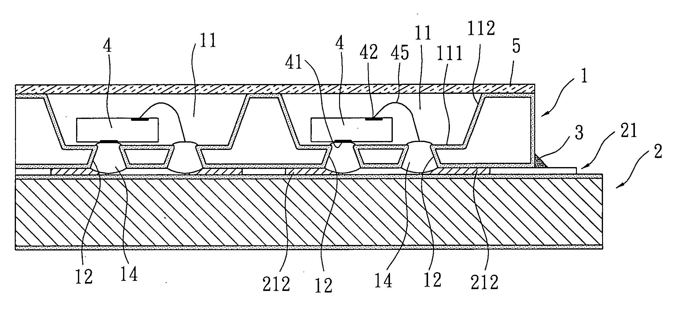
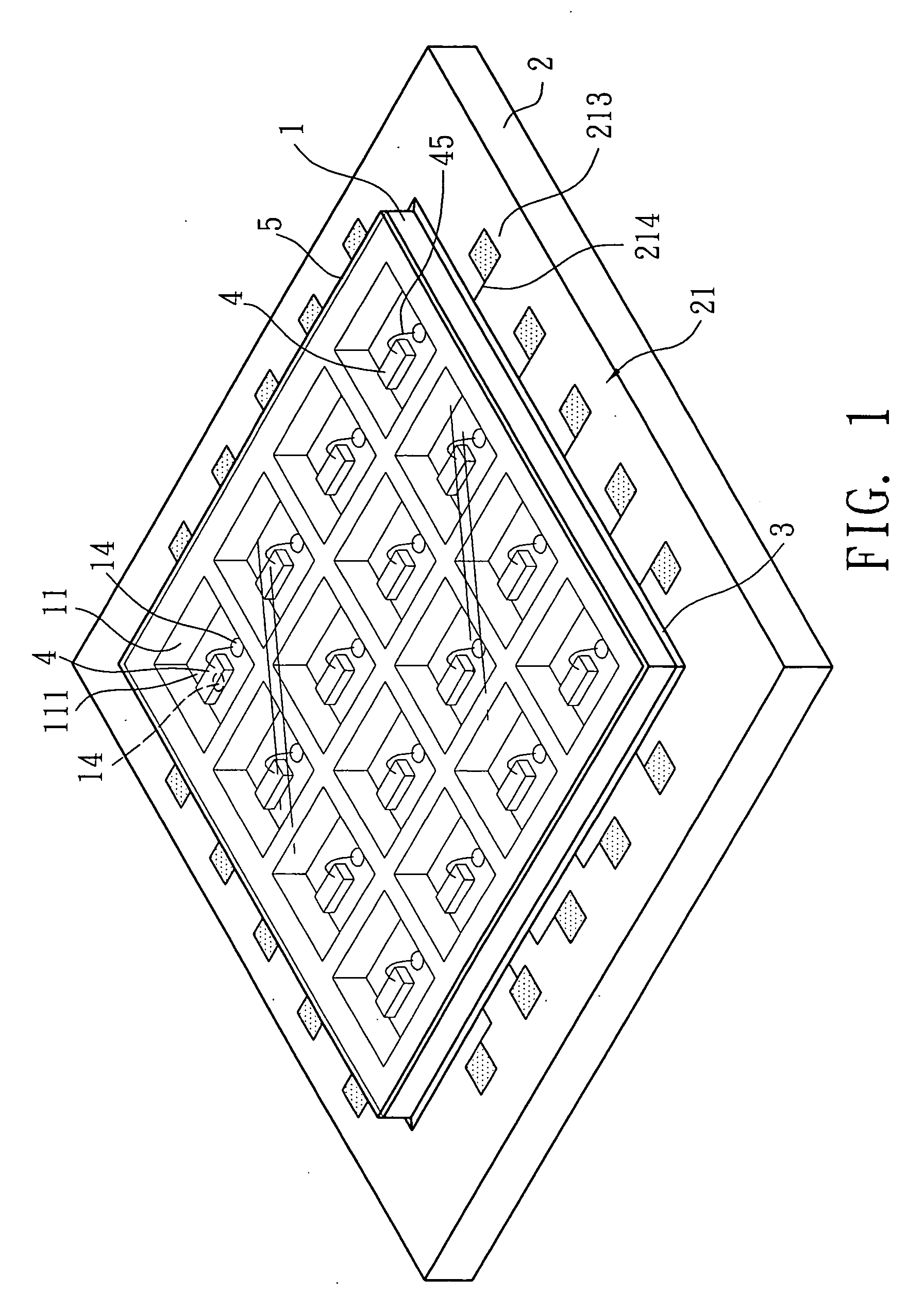
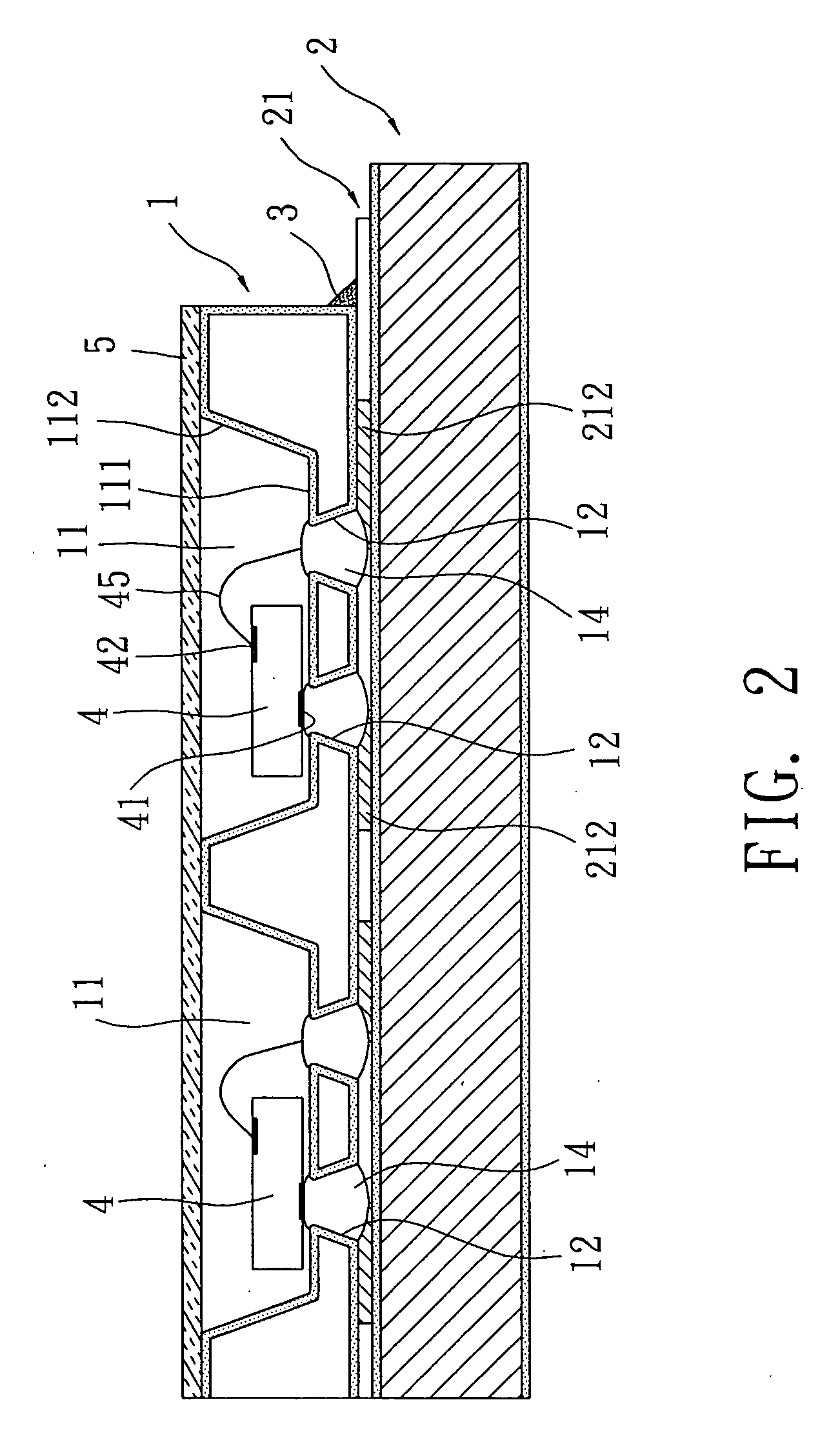
[0035] Please refer to FIGS. 1 to 3. The array-type modularized light-emitting diode structure of the present invention includes a lower substrate 2 and an upper substrate 1 fixed on a surface of the lower substrate 2.

[0036] The upper substrate 1 has a certain high heat conductivity. Multiple arrayed dents 11 are formed in the upper substrate 1. In this embodiment, multiple dents 11 are formed in the upper substrate 1 and arranged in a 4×4 array. Each dent 11 has a wall 112 inclined by a certain angle, whereby the dent 11 is tapered for enhancing reflection effect. Alternatively, the wall 112 of the dent 11 can be vertical or round. Each dent 11 has a bottom 111 formed with at least two through holes 12 passing through the bottom 111. A conductive material 14 is disposed in each through hole 12. At least one light-emitting diode crystallite 4 is fixed on the bottom 111 of each dent 11. Each light-emitting diode crystallite 4 has two electrodes 41, 42. The dents 11 of the upper subs...


PUM

PropertyMeasurementUnit
heat conductivityaaaaaaaaaa
conductiveaaaaaaaaaa
transparencyaaaaaaaaaa

Abstract

An array-type modularized light-emitting diode structure and a method for packaging the structure. The array-type modularized light-emitting diode structure includes a lower substrate and an upper substrate fixed on the lower substrate. A material with high heat conductivity is selected as the material of the upper substrate. The upper substrate is formed with multiple arrayed dents and through holes on the bottom of each dent. A material with high heat conductivity is selected as the material of the lower substrate. The surface of the lower substrate is formed with a predetermined circuit layout card. The bottom face of the upper substrate is placed on the upper face of the lower substrate with the through holes of the dents respectively corresponding to the contact electrodes of the circuit layout card of the lower substrate. Multiple light-emitting diode crystallites are respectively fixed on the bottoms of the dents. Via the through holes, the electrodes of the light-emitting diode crystallites are electrically connected with the contact electrodes. Then the dents of the upper substrate are sealed to prevent the light-emitting diode crystallites from being oxidized.

Description

BACKGROUND OF THE INVENTION [0001] The present invention is related to an array-type modularized light-emitting diode structure and a method for packaging the structure. In the modularized light-emitting diode structure, multiple light-emitting diodes are arranged in an array. [0002]FIG. 14 shows the packaging structure of a conventional light-emitting diode. The bottom electrode 61 of the light-emitting diode crystallite 6 is electrically adhered to a first metal electrode layer 62. The top electrode 61 of the light-emitting diode crystallite 6 via a conductive wire 66 is connected to another first metal electrode layer 62. The two first metal electrode layers 62 are both disposed on upper face 71 of a fiberglass substrate 7 and respectively connected to two second metal electrode layers 63 under lower face 73 of the fiberglass substrate 7 through perforations 72. Each light-emitting diode crystallite 6 is surrounded by a bowl-shaped reflective board 64 for focusing and upward refl...

Claims


Application Information

Patent Timeline
Patent Type & Authority Applications(United States)
IPC IPC(8): H01L29/06H01L33/48H01L33/62H01L33/64
CPCH01L24/73H01L25/0753H01L2924/10253H01L2924/12041H01L2924/16195H01L2924/15165H01L2224/73265H01L33/486H01L33/62H01L33/641H01L2224/48091H01L2924/00014H01L2924/15153H01L2924/00H01L2924/351
Inventor TSOU, CHING-FUCHEN, I-JUCHAO, YEH-CHIN
Owner TSOU CHING FU
Why Eureka
Try Eureka