

Method and apparatus for RFID device assembly
a technology of rfid devices and assembly methods, which is applied in the direction of semiconductor devices, electrical apparatus, basic electric elements, etc., can solve the problems of reducing the accuracy required for chip placement, increasing the cost of rfid tags, and increasing the difficulty of interconnection with other device components, e.g. antennas,
- Summary
- Abstract
- Description
- Claims
- Application Information
AI Technical Summary
Benefits of technology
Problems solved by technology
Method used
Image

Examples
Embodiment Construction
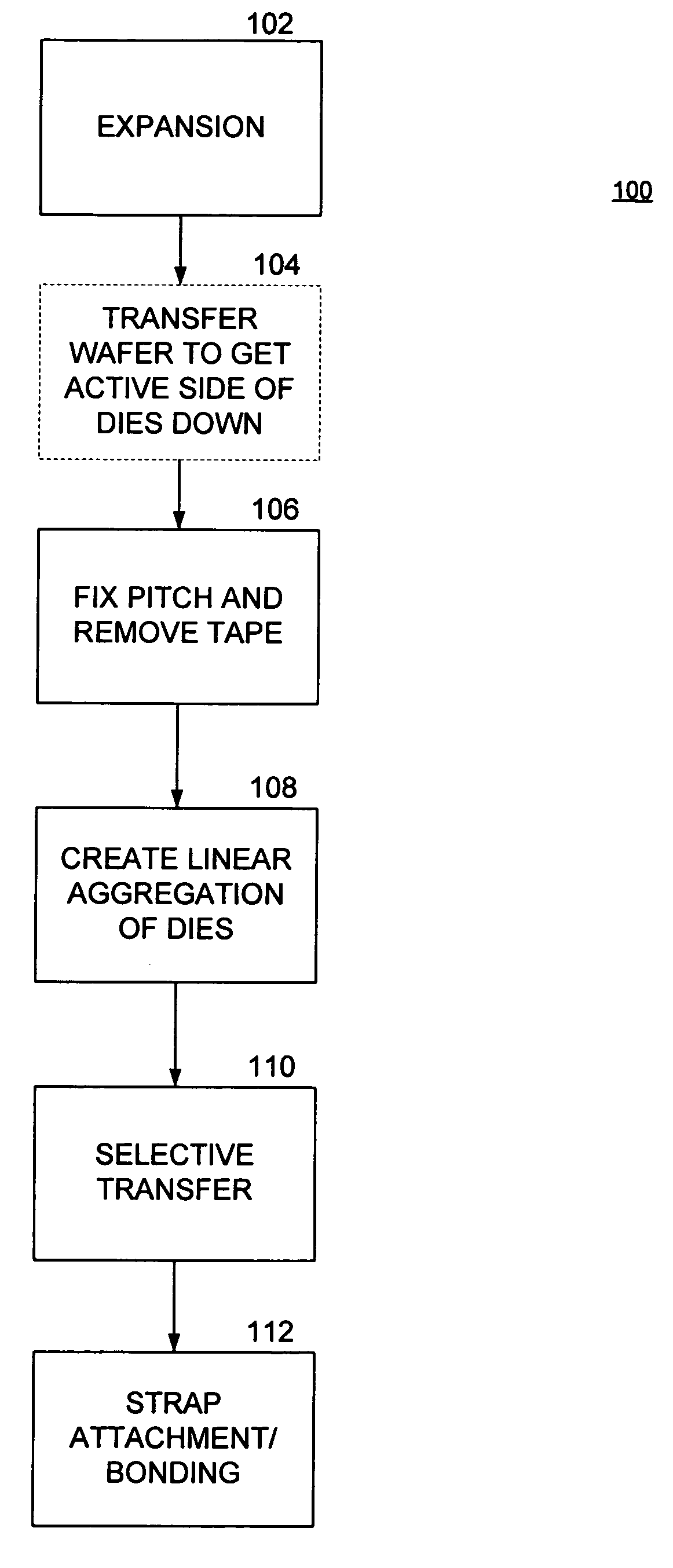
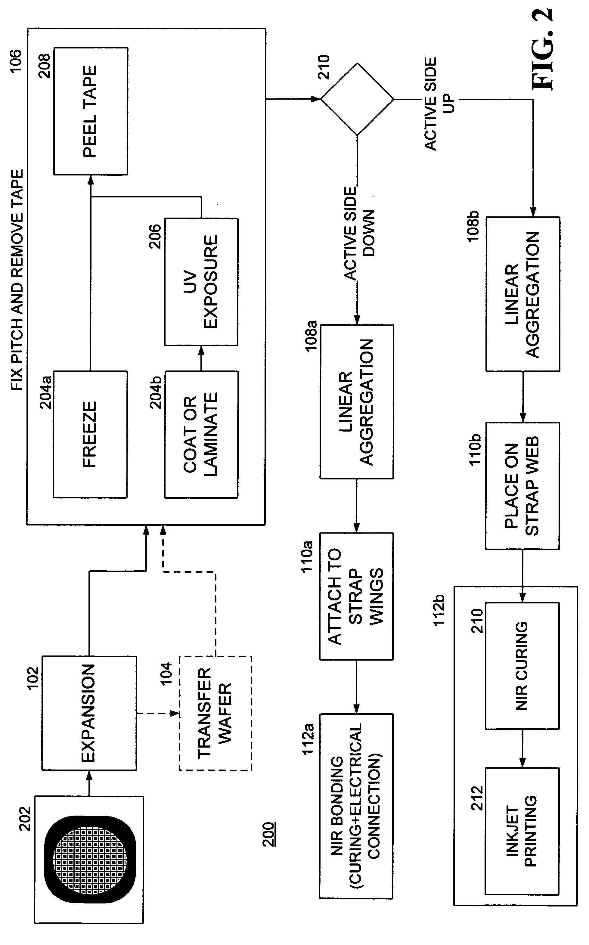
[0009] In accordance with the various exemplary embodiments thereof described herein, a process for creating semiconductor devices, such as RFID assemblies, begins with the provision of an array of semiconductor dies mounted to a substrate and spaced apart at a first pitch, or spacing. For example, a diced semiconductor wafer attached to a wafer sawing, or UV (“blue”) tape is provided in one embodiment. The substrate is stretched in so that the pitch of the dies in one direction matches a pitch between the straps in a plurality of straps. The relative positions of the dies are then fixed to a solidifiable material. The solidified material is cut into strips along a direction parallel to the direction along which the dies are stretched. Each strip, or linear aggregation of dies, is then placed using an assembly machine on a corresponding plurality of straps disposed on a strap web, and the dies contained thereon are electrically coupled to respective ones of the straps. In one embodi...
PUM
 Abstract
Description
Claims
Application Information