

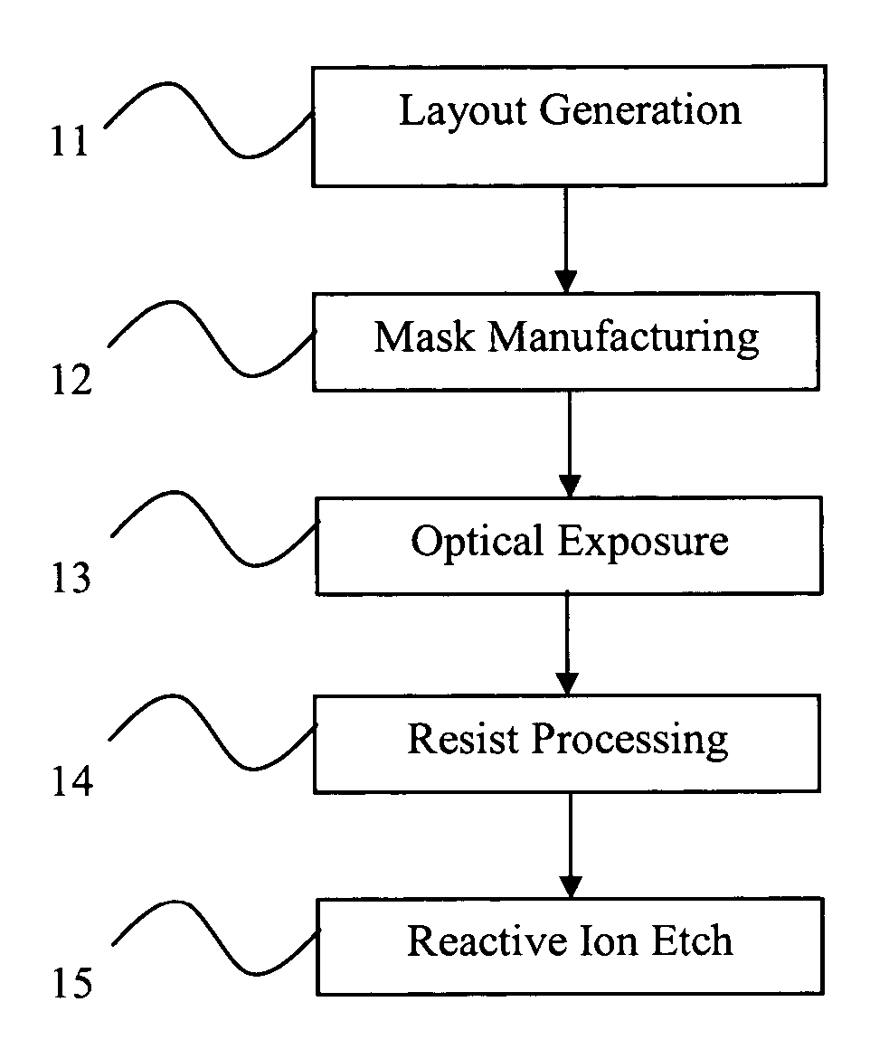
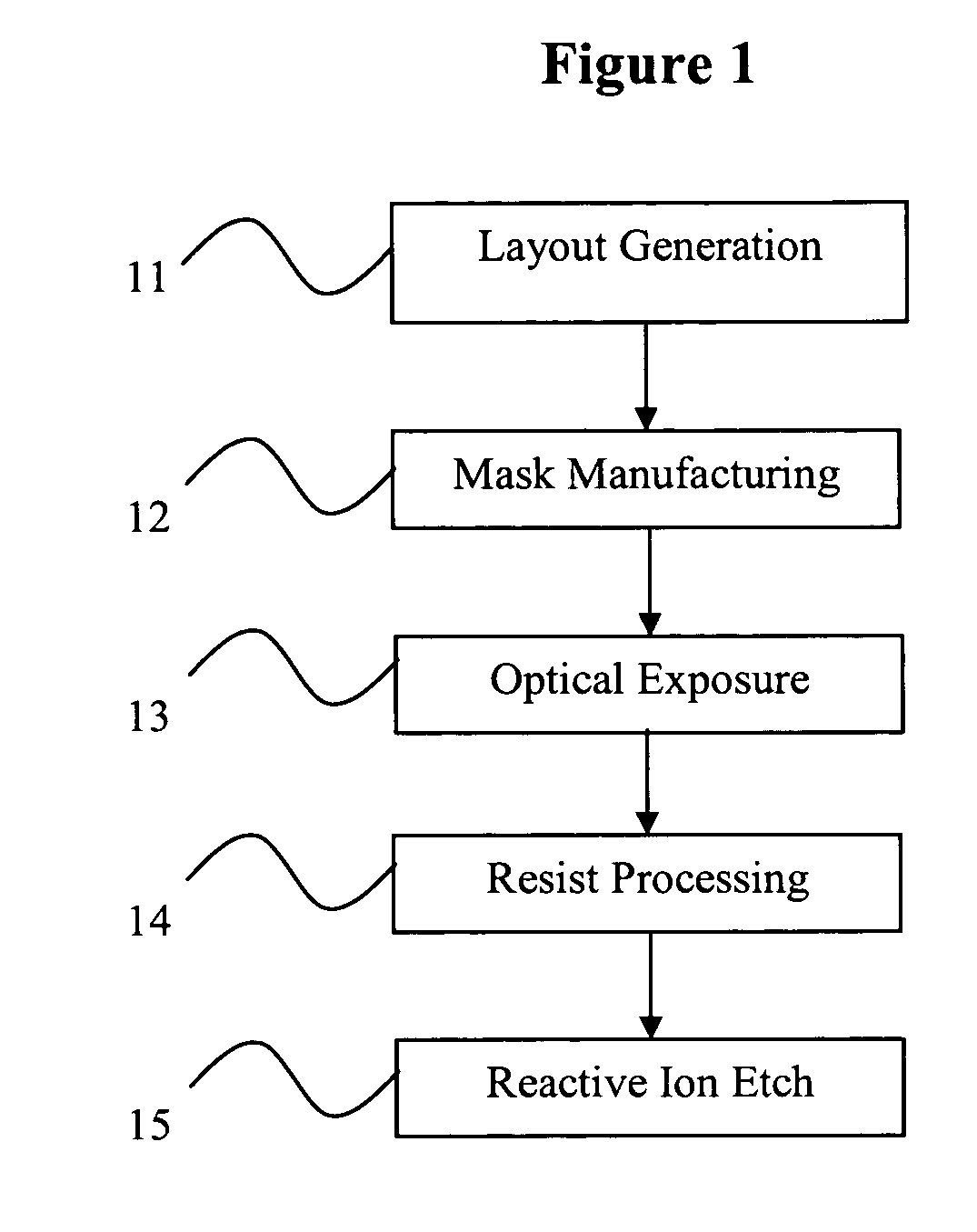
Calibration on wafer sweet spots
a lithography and sweet spot technology, applied in the field of semiconductor devices, can solve the problems of small variations in the solubility of exposed areas, affecting the exact shape of resist patterns, and non-uniformities in any one of these parameters across the wafer, and achieve the effect of accurate modeling
- Summary
- Abstract
- Description
- Claims
- Application Information
AI Technical Summary
Benefits of technology
Problems solved by technology
Method used
Image

Examples
Embodiment Construction
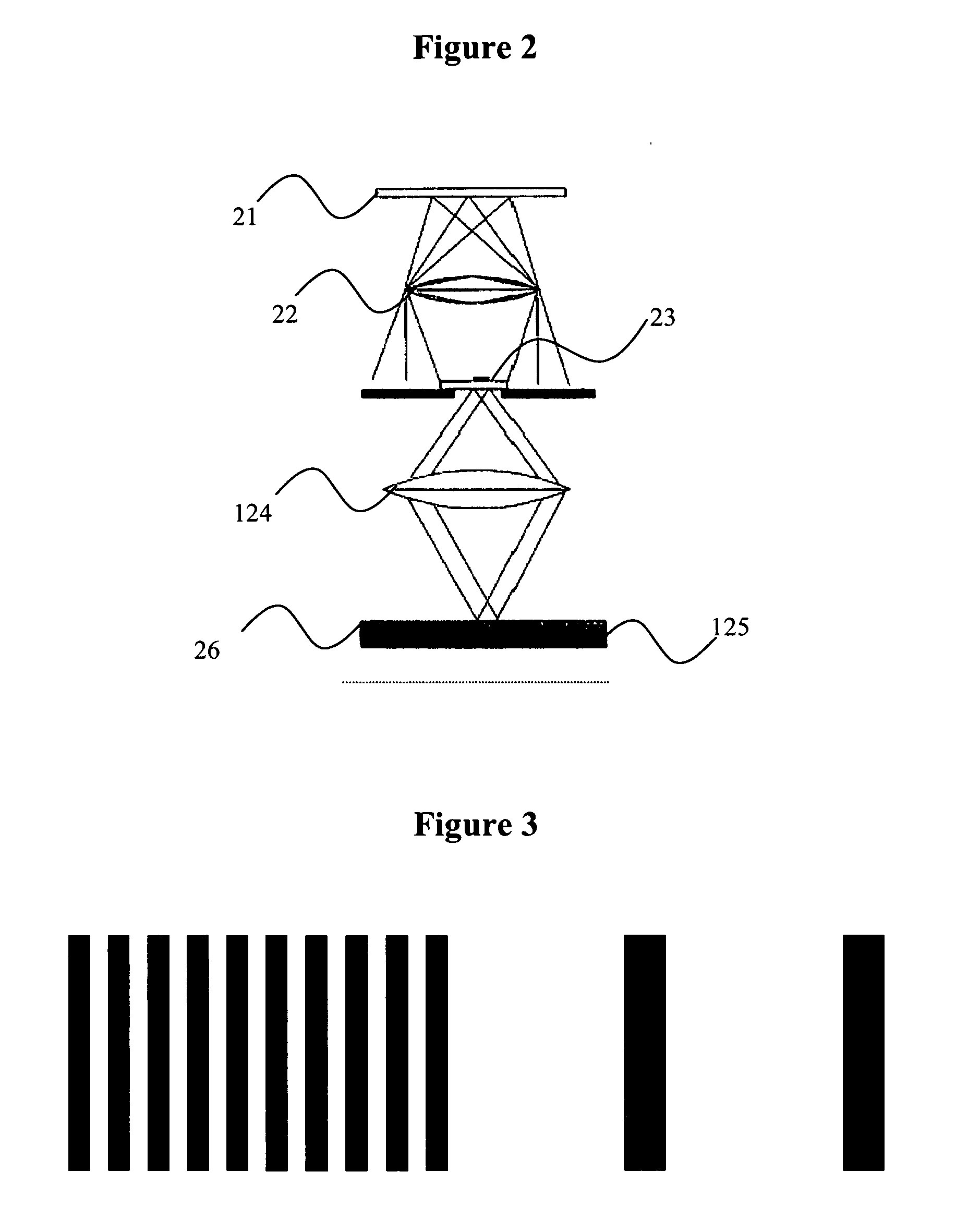
[0085] Before describing in detail embodiments that are in accordance with the present invention, it should be observed that the embodiments reside primarily in combinations of method steps related to calibration of computational models of lithography applied during the process of fabricating a semiconductor chip. Accordingly, the method steps have been represented where appropriate by conventional symbols in the drawings, showing only those specific details that are pertinent to understanding the embodiments of the present invention so as not to obscure the disclosure with details that will be readily apparent to those of ordinary skill in the art having benefit of the description herein. The terms “comprises”, “comprising”, or any other variations thereof, are intended to cover a non-exclusive inclusion, such that a process, method that comprises a list of steps does not include only those steps but may include other steps not expressly listed or inherent to such process, method. ...
PUM
 Abstract
Description
Claims
Application Information