Fast settling, low noise, low offset operational amplifier and method

Active Publication Date: 2006-11-30
TEXAS INSTR INC
View PDF11 Cites 13 Cited by
  • Summary
  • Abstract
  • Description
  • Claims
  • Application Information

AI Technical Summary

Benefits of technology

[0015] It is an object of the invention to provide a low noise operational amplif

Problems solved by technology

However, the resistive load resistors cannot provide sufficiently high voltage gain and often are replaced by active load devices, typically transistors of a current mirror circuit or other symmetrical current source circuitry.
There is a problem associated with the circuit shown in FIG. 2, in that the combination of common mode feedback between the inpu

Method used


Image

  • Fast settling, low noise, low offset operational amplifier and method
  • Fast settling, low noise, low offset operational amplifier and method
  • Fast settling, low noise, low offset operational amplifier and method

Examples


Embodiment Construction

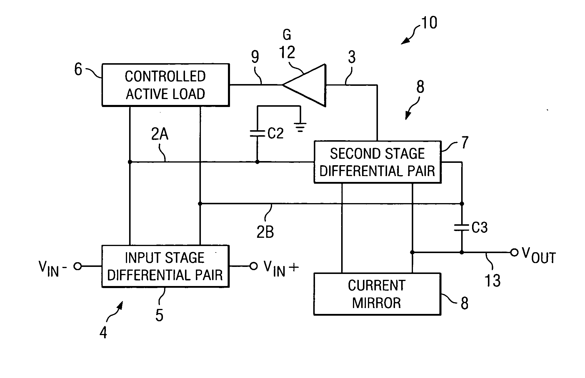
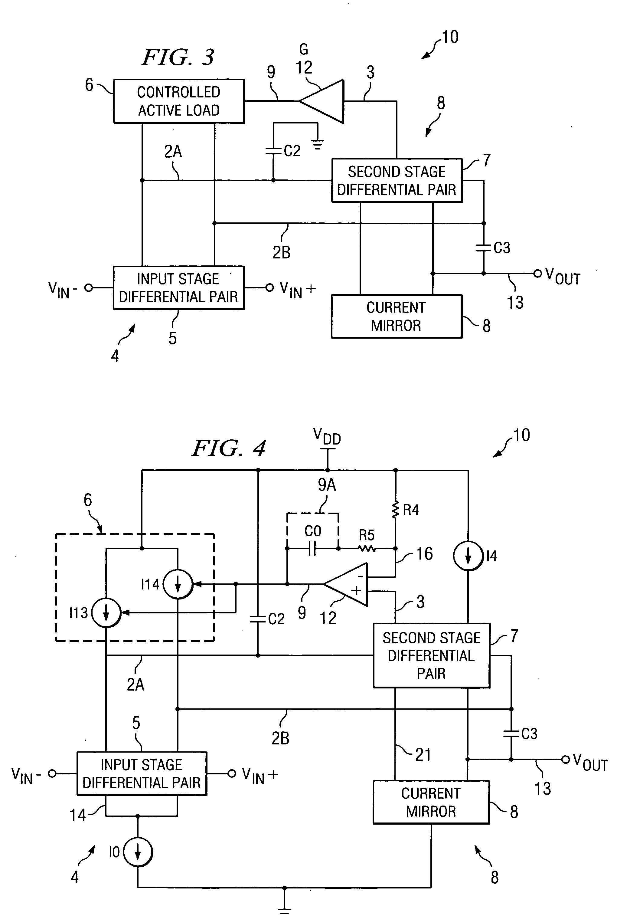
[0034]FIG. 3 shows a block diagram of a general solution to the above-mentioned slow settling problem of prior art low offset, low noise operational amplifiers. In FIG. 3, the illustrated block diagram of an operational amplifier 10 of the present invention is similar to the block diagram of prior art FIG. 2, except that a common mode feedback gain circuit 12 having a gain G has an input connected to receive the common mode feedback signal produced on conductor 3 by second stage differential pair 7 and produces an amplified common mode feedback signal on conductor 9. Conductor 9 applies the amplified common mode feedback signal to a control input of controlled active load circuit 6. As in prior art FIG. 2, controlled active load circuit 6 is coupled by conductors 2A and 2B to collectors or drains of input transistors of input stage differential transistor pair 5, inputs of which are coupled to Vin− and Vin+. Conductor 2A is connected to one terminal of compensation capacitor C2 and ...


PUM


Abstract

An amplifier (10) includes a first stage (4) including differentially coupled first (Q1) and second (Q2) input transistors and a controlled active load circuit (6). A second stage (8) includes differentially coupled third (Q5) and fourth (Q6) input transistors and a load circuit (Q7,8). A first output (2A) of the first stage (4) is coupled to a first input of the second stage (8), a second output (2B) of the first stage (4) being coupled to a second input of the second stage (8). A common mode feedback amplifier (12) has an input coupled to receive a common mode signal (3) from the second stage (8) for producing an amplified common mode signal (9) on a control input of the controlled active load circuit (6) to provide fast settling of an output (Vout) of the second stage without substantially increasing amplifier noise.

Description

BACKGROUND OF THE INVENTION [0001] The present invention relates generally to amplifiers, and more particularly to low noise operational amplifiers having fast settling of the output signal and low input offset voltages. [0002] To achieve low noise in operational amplifiers, it is necessary to minimize the number of circuit elements that contribute noise in the first stage (i.e., the input stage) of the operational amplifier. Typically, the main noise contributors are the two input transistors which constitute the differential input transistor pair of the input stage. In addition to the input transistors, the input stage of a typical low noise operational amplifier also contains load devices, which typically are large-value resistors. However, the resistive load resistors cannot provide sufficiently high voltage gain and often are replaced by active load devices, typically transistors of a current mirror circuit or other symmetrical current source circuitry. In order to minimize noi...

Claims


Application Information

Patent Timeline
IPC IPC(8): H03F3/45
CPCH03F1/48H03F3/45085H03F2203/45014H03F2203/45086H03F2203/45248H03F2203/45712H03F2203/45441H03F2203/45632H03F2203/45642H03F2203/45646H03F2203/45652H03F2203/45431
Inventor ALENIN, SERGEY V.SURTIHADI, HENRY
Owner TEXAS INSTR INC
Why Eureka
Try Eureka