MOS transistor device structure combining Si-trench and field plate structures for high voltage device

a transistor device and field plate technology, applied in the direction of transistors, semiconductor devices, electrical equipment, etc., can solve the problem of relatively large device size, achieve the effect of effective elongation of electric current path, reduce size, and improve performan

Active Publication Date: 2006-11-30
UNITED MICROELECTRONICS CORP
View PDF4 Cites 74 Cited by
  • Summary
  • Abstract
  • Description
  • Claims
  • Application Information

AI Technical Summary

Benefits of technology

[0010] It is an object of the present invention to provide an improved HV MOS transistor device, which has a reduced device size.
[0011] It is another object of the present invention to provide a method of manufacturing the improved HV MOS transistor device having a reduced device size.
[0015] The HV MOS device of the present invention includes a plurality of protrusions of the field oxide region extending to the deep well and a plurality of field plates on or in the field oxide region between the gate and the drain or source, effectively elongating the electric current path between the gate and the drain or source. Accordingly, the HV MOS device has a reduced size with an improved performance.

Problems solved by technology

While, to achieve a good improvement of the breakdown voltage, a certain width is needed for the field oxide region and the resulting size of the device is relatively large.

Method used


Image

  • MOS transistor device structure combining Si-trench and field plate structures for high voltage device
  • MOS transistor device structure combining Si-trench and field plate structures for high voltage device
  • MOS transistor device structure combining Si-trench and field plate structures for high voltage device

Examples


Embodiment Construction

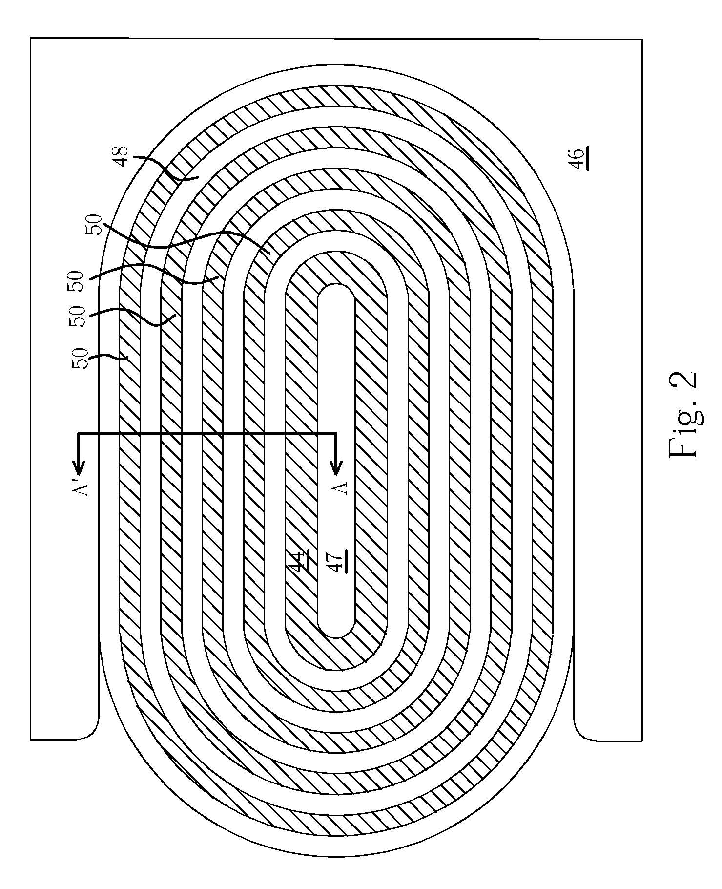
[0024] The present invention is more described in detail by the embodiments set forth as follows. FIGS. 2 and 3 show an embodiment of the high voltage NMOS transistor device according to the present invention. FIG. 2 shows a top view and FIG. 3 shows a cross-sectional view taken along line A-A′ of FIG. 2. It is understood that the charge properties shown in figures are exemplary, and suitable modification of the polarities can be made to form a super high voltage PMOS transistor device.

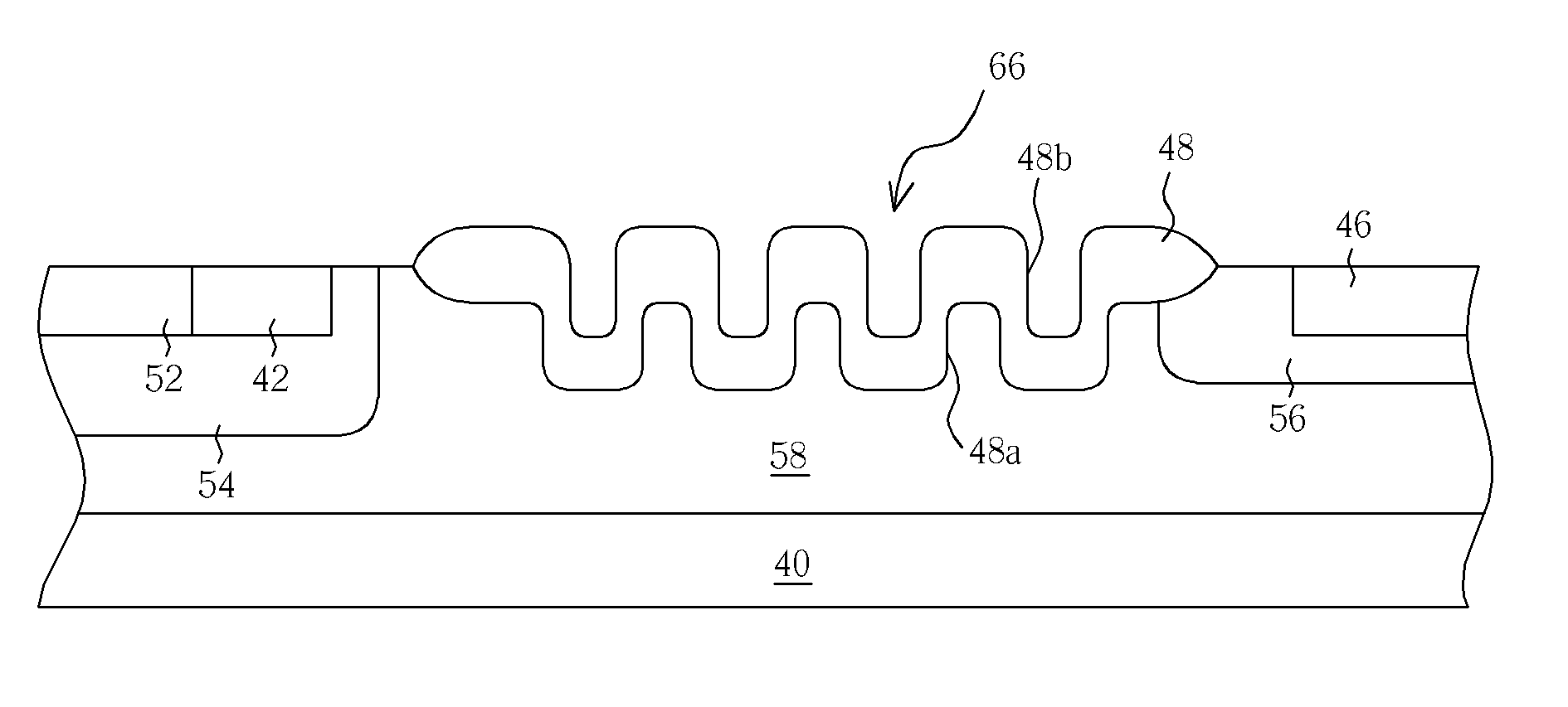
[0025] The super high voltage NMOS transistor device 2 is formed on a semiconductor substrate 40 and includes a source diffusion region 42, a drain diffusion region 46, and a gate 44. A gate dielectric layer 47 is formed between the source diffusion region 42 and the gate 44. The gate 44 may be made of polysilicon or metals and is isolated from the drain 46 with a long pass isolation 48 therebetween. The long pass isolation 48 is a field oxide region and a lower surface of the long pass isolation 48 ...


PUM


Abstract

A metal-oxide-semiconductor transistor device for high voltage (HV MOS) and a method of manufacturing the same are disclosed. The HV MOS transistor device comprises a field oxide region with an indented lower surface combined with a plurality of field plates to elongate the path for disturbing the lateral electric field, therefore the transistor device has a relatively small size.

Description

CROSS REFERENCE TO RELATED APPLICATIONS [0001] This application claims priority from U.S. provisional application No. 60 / 594,987 by Chen et al., filed May 25, 2005, entitled “Super HV LDMOS device structure-combination of Si-trench and field plate structures”.BACKGROUND OF THE INVENTION [0002] 1. Field of the Invention [0003] The present invention relates to super high voltage semiconductor devices and, more particularly, to a high voltage metal-oxide-semiconductor (HV MOS) transistor device having a structure of a combination of trench and field plate structures. [0004] 2. Description of the Prior Art [0005] In current semiconductor processing, controllers, memories, circuits of low-voltage operation and power devices of high-voltage operation are largely integrated into a single chip to achieve a single-chip system. The power device, such as vertical double-diffusion metal-oxide-semiconductor (VDMOS), insulated gate bipolar transistor (IGBT) and lateral diffused MOS (LDMOS), is em...

Claims


Application Information

Patent Timeline
Patent Type & Authority Applications(United States)
IPC IPC(8): H01L29/76H01L21/336
CPCH01L29/0619H01L29/0878H01L29/407H01L29/7823H01L29/66681H01L29/7816H01L29/42368
Inventor CHEN, LI-CHEWANG, CHIH-CHONG
Owner UNITED MICROELECTRONICS CORP
Why Eureka
Try Eureka