Semiconductor light emitting device

Active Publication Date: 2006-12-07
ROHM CO LTD
View PDF7 Cites 137 Cited by
  • Summary
  • Abstract
  • Description
  • Claims
  • Application Information

AI Technical Summary

Benefits of technology

[0021] The transparent electrode preferably comprises a Zn1-xMgxO (wherein 0≦x<1) film. Zn1-xMgxO (wherein 0≦x<1 and, when x=0, ZnO) provides excellent ohmic contact with a GaN semiconductor layer, and has a transmittance

Problems solved by technology

However, it is necessary to provide the P-side and N-side electrodes on the InGaN semiconductor light emitting portion and route wires from the electrodes, because the sapphire substrate is insulative.
Therefore, light from the InGaN semiconductor light emitting po

Method used


Image

  • Semiconductor light emitting device
  • Semiconductor light emitting device
  • Semiconductor light emitting device

Examples


Embodiment Construction

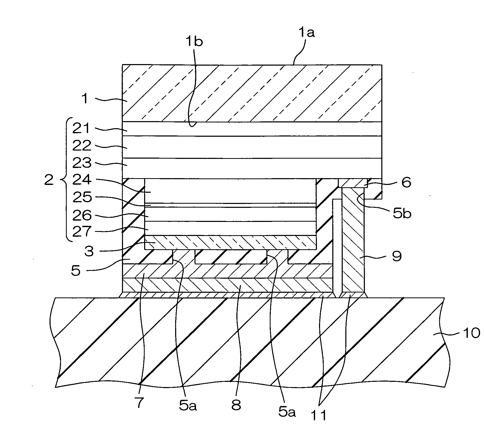
[0030]FIG. 1 is a sectional view schematically illustrating the construction of a light emitting diode element according to one embodiment of the present invention. The light emitting diode element is of a flip-chip type, and includes a sapphire substrate 1 as a transparent substrate, an InGaN semiconductor light emitting portion 2 provided on the sapphire substrate 1, and a P-side transparent electrode 3 covering a surface of the InGaN semiconductor light emitting portion 2 opposite from the sapphire substrate 1. The sapphire substrate 1 has a light extracting surface 1a defined by one surface thereof and a device formation surface 1b defined by the other surface thereof. The InGaN semiconductor light emitting portion 2 is provided on the device formation surface 1b.

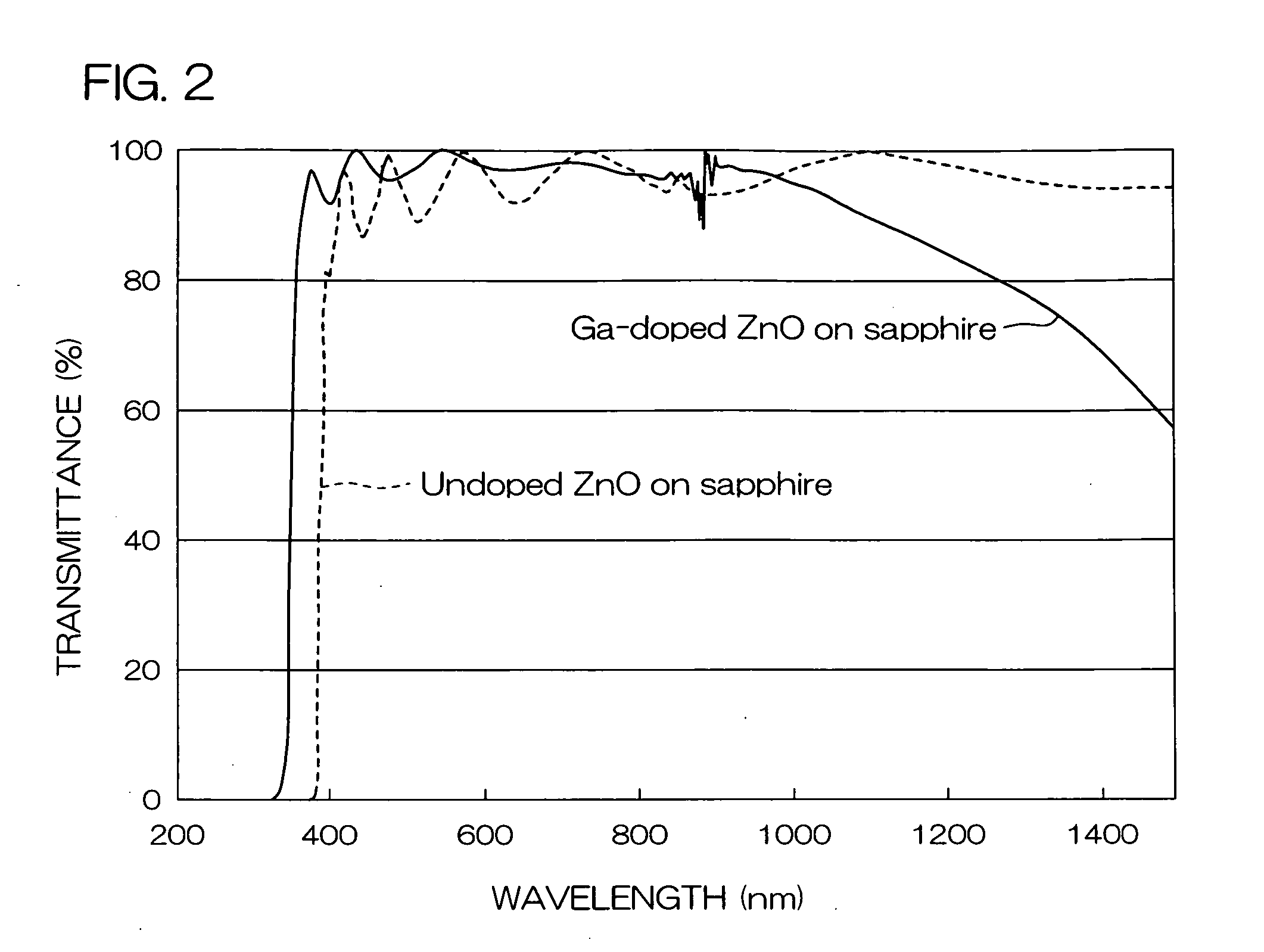
[0031] The sapphire substrate 1 is an insulative substrate which is transparent to the wavelength (e.g., 460 nm) of light emitted from the InGaN semi conductor light emitting portion 2. The InGaN semiconductor light em...


PUM


Abstract

A semiconductor light emitting device includes a semiconductor light emitting portion having a first contact layer of a first conductivity, a second contact layer of a second conductivity and an active layer sandwiched between the first and second contact layers. The device further includes a transparent electrode which substantially entirely covers a surface of the second contact layer in ohmic contact with the surface of the second contact layer and is transparent to a wavelength of light emitted from the semiconductor light emitting portion, and a metal reflection film which is opposed to substantially the entire surface of the transparent electrode and electrically connected to the transparent electrode, and reflects the light emitted from the semiconductor light emitting portion and passing through the transparent electrode toward the semiconductor light emitting portion.

Description

TECHNICAL FIELD [0001] The present invention relates to a semiconductor light emitting device such as a gallium nitride light emitting diode. BACKGROUND ART [0002] A blue light emitting diode element, for example, includes an InGaN semiconductor light emitting portion provided on a surface of a sapphire substrate, and electrodes respectively provided on P- and N-sides of the InGaN semiconductor light emitting portion (see Patent Document 1 listed below). However, it is necessary to provide the P-side and N-side electrodes on the InGaN semiconductor light emitting portion and route wires from the electrodes, because the sapphire substrate is insulative. Therefore, light from the InGaN semiconductor light emitting portion is blocked by the electrodes and the like, so that the light extraction efficiency is low. [0003] This problem is alleviated by employing a flip-chip structure in which the InGaN semiconductor light emitting portion is bonded to a mounting board in opposed relation t...

Claims


Application Information

Patent Timeline
IPC IPC(8): H01L33/00H01L33/22H01L33/40H01L33/42H01L33/44H01L33/62
CPCH01L33/22H01L33/405H01L33/42H01L33/44H01L2924/0002H01L33/62H01L2924/00
Inventor ASAHARA, HIROKAZUSAKAI, MITSUHIKOSONOBE, MASAYUKINISHIDA, TOSHIO
Owner ROHM CO LTD
Why Eureka
Try Eureka