Organic electroluminescence display apparatus

a display apparatus and electroluminescence technology, applied in the direction of discharge tube luminescnet screen, discharge tube/lamp details, organic semiconductor devices, etc., can solve the problem of high specific resistance of ito film, the inability to achieve high light emission efficiency, and the reduction of the light emission area per pixel. , to achieve the effect of low specific resistan

Inactive Publication Date: 2006-12-07
FUJIFILM CORP
View PDF3 Cites 35 Cited by
  • Summary
  • Abstract
  • Description
  • Claims
  • Application Information

AI Technical Summary

Benefits of technology

[0028] A first aspect of the present invention provides an organic electroluminescence display apparatus. The organic electroluminescence display apparatus comprises a first substrate and a second substrate adhered to the first substrate. The first substrate comprises a first base substrate having an organic electroluminescence device that comprises a first electrode, an organic electroluminescence layer, and a second electrode provided in this order from the first base substrate. The second substrate comprises a second base substrate and a patterned conductive film with a lower specific resistance than the second electrode. The patterned conductive film is provided on the side of the second base substrate which side is near to the first substrate. The conductive film is electrically connected to the second electrode.

Problems solved by technology

As described above, in the case of a bottom emission type display apparatus, the light generated in the organic electroluminescence device is taken out from the insulating substrate side; thus if a switching element is formed between the insulating substrate and the organic electroluminescence device, the switching element becomes a light shielding element, which results in substantial reduction in the light emission area per 1 pixel due to the presence of the switching element, thus presenting a problem in that a high light emission efficiency cannot be obtained.
In this case, in order to provide the cathode with an optical transparency, a transparent conductive film, such as an ITO film, is used; however, the ITO film presents a problem of high specific resistance.
In addition, optical transparency can be obtained by reducing the thickness of the Ag film, preferably to a thickness of 20 nm or less; however, such a reduction in thickness presents a problem in that a low resistance film cannot be obtained.
Such an increase in resistance of the cathode accompanying increased optical transparency results in an increased voltage drop across the cathode, which causes a problem that, with the size of the organic electroluminescence display apparatus being increased, the non-uniformity in brightness gets worse.

Method used


Image

  • Organic electroluminescence display apparatus
  • Organic electroluminescence display apparatus
  • Organic electroluminescence display apparatus

Examples


example 2

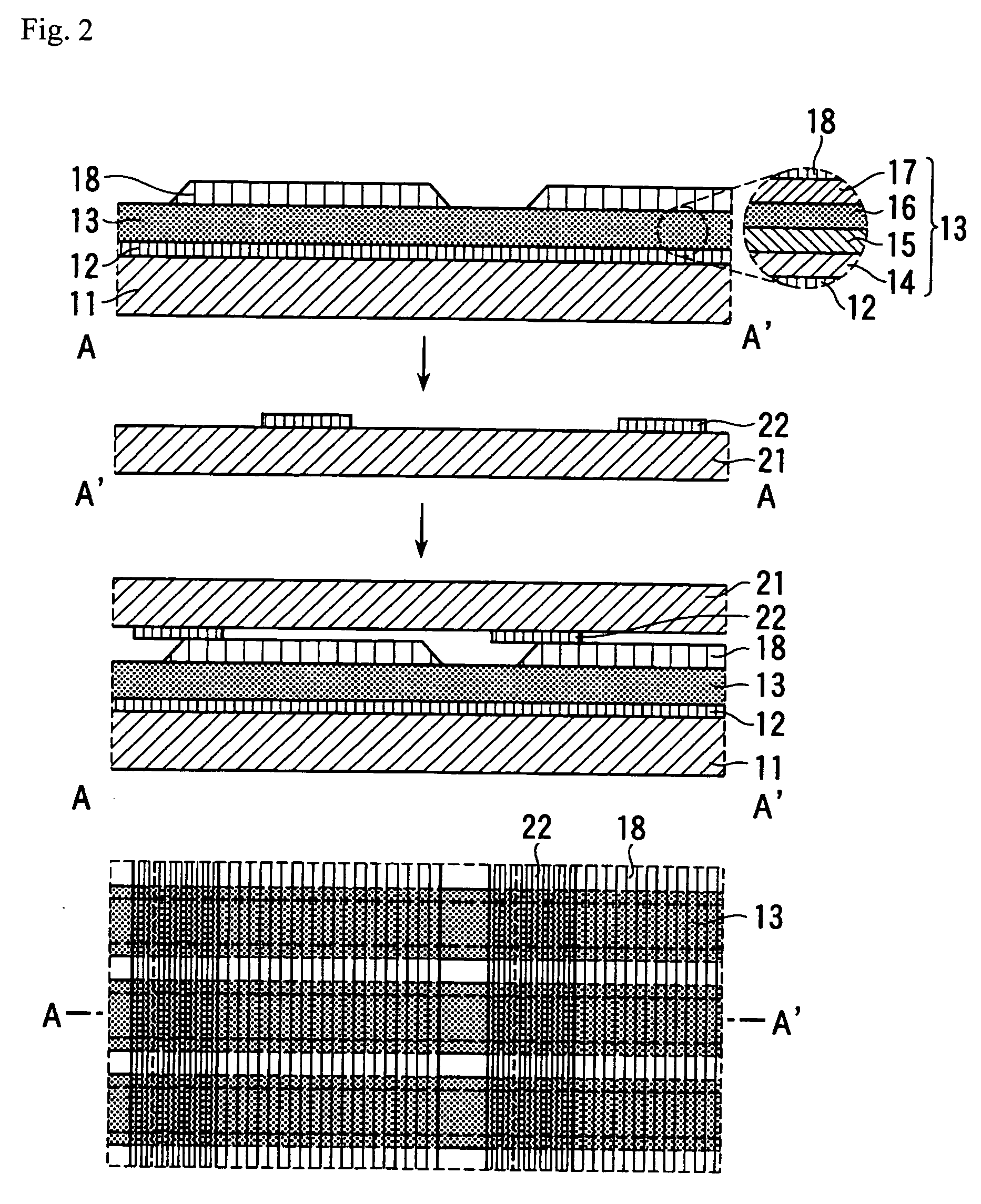
[0062] Next, with reference to FIG. 3, a top emission type display apparatus using an organic EL device according to EXAMPLE 2 of the present invention will be described.

[0063]FIG. 3 is a schematic cross-sectional view of substantial portions of a top emission type display apparatus using an organic EL device according to EXAMPLE 2 of the present invention, in which a convex insulating film 19 made of a photosensitive polyimide is formed, resulting in a sectional geometry which is different from that in EXAMPLE 1. However, the manufacturing processes other than the formation of the insulating film 19 is the same as those in EXAMPLE 1. In addition, the other signs indicate the same members as those in FIG. 2.

[0064] Also in EXAMPLE 2, the aperture ratio can be increased as in EXAMPLE 1, and the reduction in manufacturing yield can be suppressed.

example 3

[0065] Next, with reference to FIG. 4, a top emission type display apparatus using an organic EL device according to EXAMPLE 3 of the present invention will be described. FIG. 4 is a schematic cross-sectional view of substantial portions of a top emission type display apparatus using an organic EL device according to EXAMPLE 3 of the present invention, in which a black matrix 23 made of a black resin is provided between the second glass base substrate 21 and the auxiliary electrode 22. The manufacturing processes other than the formation of the black matrix 23 are the same as that in EXAMPLE 1. In addition, the other signs indicate the same members as those in FIG. 2.

[0066] In this case, in order to avoid electrical connection between adjacent stripes of the cathode 18 in adhering the first glass base substrate 11 to the second glass base substrate 21, the auxiliary electrode 22 on the black matrix 23 has a width narrower than that of the black matrix 23, and is formed at a positio...

example 4

[0068] Next, with reference to FIG. 5, a top emission type display apparatus using an organic EL device according to EXAMPLE 4 of the present invention will be described. FIG. 5 is a schematic cross-sectional view of substantial portions of a top emission type display apparatus using an organic EL device according to EXAMPLE 4 of the present invention, in which a concavo-convex structure 24 is formed on the surface of the second glass base substrate 21 that is nearer to the first glass base substrate 11. The surface of the auxiliary electrode 22 that is on the display surface side is provided with a concavo-convex structure owing to the concavo-convex structure 24. The manufacturing processes other than the formation of the concavo-convex structure 24 are the same as that in EXAMPLE 1. In addition, the other signs indicate the same members as those in FIG. 2.

[0069] The concavo-convex structure 24 in this case is formed by coating the second glass base substrate 21 with a photosensi...


PUM


Abstract

An organic electroluminescence display apparatus comprising a first substrate 101 and a second substrate 102 adhered to the first substrate, wherein the first substrate 101 comprises a first base substrate 1 having an organic electroluminescence device 2, the organic electroluminescence device 2 comprises a first electrode 3, an organic electroluminescence layer 4, and a second electrode 5 provided in this order from the first base substrate side, the second substrate 102 comprises a second base substrate 6 and a patterned conductive film 7 provided on the second base substrate 6 such that the patterned conductive film 7 faces the first substrate 101, the patterned conductive film 7 has a lower specific resistance than the second electrode 5, and the conductive film 7 is electrically connected to the second electrode 5.

Description

CROSS-REFERENCE TO RELATED APPLICATION [0001] This application claims priority under 35 USC 119 from Japanese patent Application Nos. 2005-140624, the disclosure of which is incorporated by reference herein. BACKGROUND OF THE INVENTION [0002] 1. Field of the Invention [0003] The present invention relates to an organic electroluminescence display apparatus, and particularly relates to an organic electroluminescence display apparatus in which the display surface is provided on the side opposite to the substrate, and which at least features a configuration to enhance the aperture ratio for the organic electroluminescence display apparatus. [0004] 2. Description of the Related Art [0005] As a display apparatus which can be rendered thin-sized and lightweight, compared to the conventional CRT (cathode ray tube) and LCD (liquid crystal display), the display apparatus which uses an organic electroluminescence (EL) device has attracted a lot of attention in recent years. [0006] Because the ...

Claims


Application Information

Patent Timeline
Patent Type & Authority Applications(United States)
IPC IPC(8): H05B33/12H01L51/50
CPCH01L27/3276H01L51/5228H01L2251/5315H01L51/5268H01L51/5284H01L51/5237H10K59/131H10K50/824H10K50/8426H10K50/854H10K50/865H10K2102/3026
Inventor YAEGASHI, HIROYUKI
Owner FUJIFILM CORP
Why Eureka
Try Eureka