Optical waveguide and process for manufacturing the same

Inactive Publication Date: 2006-12-07
FUJIFILM BUSINESS INNOVATION CORP
View PDF7 Cites 19 Cited by
  • Summary
  • Abstract
  • Description
  • Claims
  • Application Information

AI Technical Summary

Benefits of technology

[0016] The present invention provides an optical waveguide having the function of significantly changing the direction of light propagation by the use of a reflecting surface comprised of an air clad within the

Problems solved by technology

Although methods of changing the direction of light propagation using various polymer waveguides are being considered, there are problems such as those described in the following (1) to (3) are imposed.
However, it is not possible to avoid a loss caused by utilization of a radiation mode when an arc is used.
However, since the difference in refractive index between a core and a clad is small, a large change in direction was not possible.
Also, complete total reflection cannot be performed and there is a leakage of light at the total reflecting surface.
However, it is impossible to carry out cutting locally.
Also, because the polymer optical waveguide is actually cut in this cutting process, it is difficult to attain this cutting at a place except for the end surface of the optical waveguide.
Also, because accuracy of the dicing position is required, leading to an increase in the number of steps as well bringing about high costs.
By this method, the reduction in leakage of light reduces the optical loss and the curvature radius can be made small; however, a limitation to miniaturization remains as before.
However, in this method, since the air clad layer is located on the exterior, the manufacturing process is complicated and the air clad cannot be easily produced.
In the configuration disclosed in JP-A No. 2003-75670, the air clad is formed by etching, but the surface formed by etching tends to be rough, giving rise to the problem that the reflecting surface has a degraded reflecting efficiency.
Further, the equipment cost for etching tends to be higher, and the et

Method used


Image

  • Optical waveguide and process for manufacturing the same
  • Optical waveguide and process for manufacturing the same
  • Optical waveguide and process for manufacturing the same

Examples


Example

Example 1

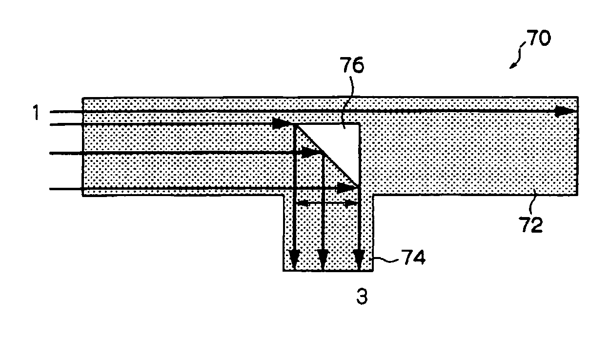
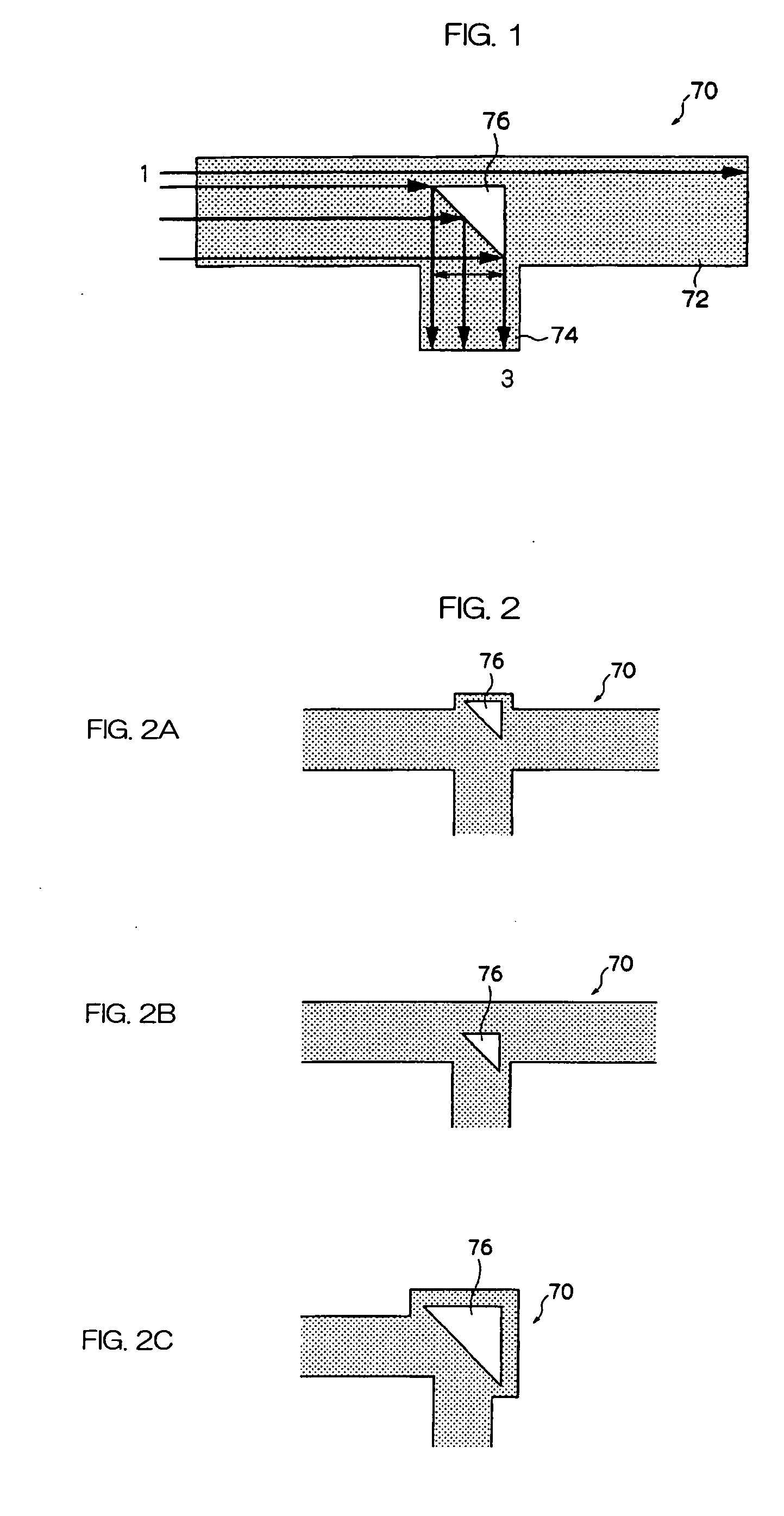
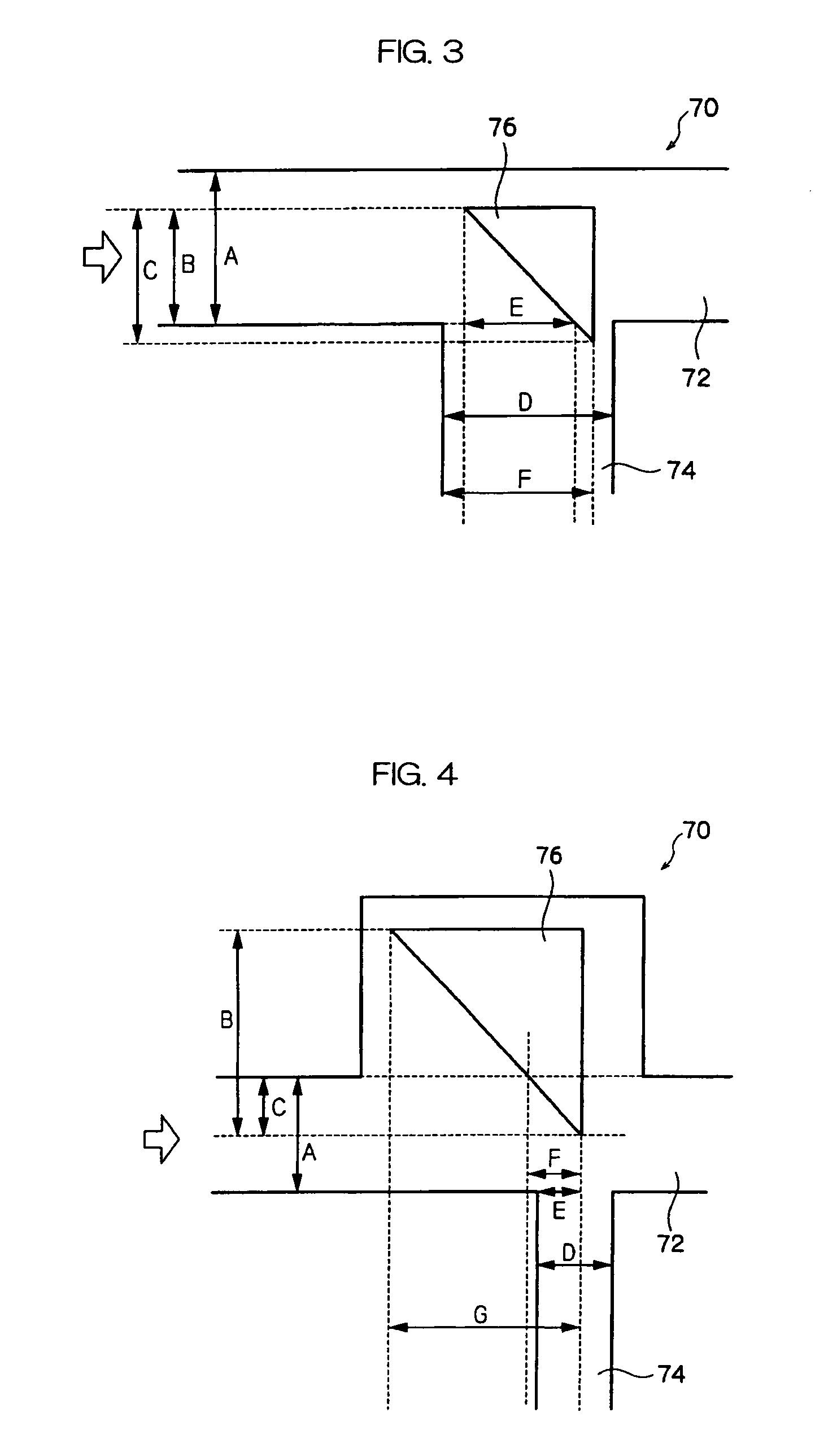
[0134] As shown in FIG. 7, a main waveguide is 100 μm by 100 μm and has a length of 20 mm, a gas cavity constituted of air has a configuration which is an isosceles triangle structure in which the sides forming a right angle are each 50 μm in length and has a plane inclined at an angle of 45° in the direction of light propagation in the main waveguide and disposed at the center of the main waveguide and a branched waveguide which is 100 μm by 100 μm and has a length of 5 mm. A ultraviolet ray-curable polymer having a refractive index of 1.54 is used for a core, a ultraviolet ray-curable polymer having a refractive index of 1.51 is used as a clad and ARTON FILM® (manufactured by JSR Corporation) is used as a bottom substrate. An LED having a wavelength of 850 nm is disposed on the incident side through a φ62.51 μm GI fiber and the light receptor side of each end part of the main waveguide, and a branched waveguide is connected to a light intensity measurer through a φ200 μm...

Example

Example 2

[0138] As shown in FIG. 8, a main waveguide is 50 μm by 50 μm and has a length of 10 mm, a gas cavity constituted of air has a configuration which is an isosceles triangle structure in which the sides forming a right angle are each 50 μm in length has a plane inclined at an angle of 45° in the direction of light propagation in the main waveguide and disposed at the center of the main waveguide and the main waveguide which extends 10 mm in the direction at an angle of 90° in the direction of the main waveguide from the border of the air part. An ultraviolet ray-curable polymer having a refractive index of 1.54 is used for a core, an ultraviolet ray-curable polymer having a refractive index of 1.51 is used as a clad and ARTON FILM® (described above) is used as a top and a bottom substrate. An LED having a wavelength of 850 nm is disposed on the incident side through a φ62.5 μm GI fiber, and the main waveguide end is connected to a light intensity measurer through a φ200 μm H...

Example

Example 3

Production of a Master Plate

[0140] As shown in FIG. 9A, a thick film resist is applied to a Si substrate 80 by a spin coating method, then pre-baked at 80° C., subjected to exposure through a photomask, and then developed to form waveguide core convex portions 82 and 84 for changing the direction of light propagation and a concave portion 86 for a cavity in a core (core width: 100 μm, cavity width: 50 cm). The substrate is post-baked at 120° C. to produce a master plate for manufacturing an optical waveguide core and a cavity in the core.

Production of a Mold

[0141] Next, after a releasing agent is applied to the master plate, a heat-curable dimethylsiloxane resin (trade name: SYLGARD184, manufactured by Dow Coning Asia Ltd.) is poured into the master plate, allowed to stand for a fixed time, then subjected to defoaming under a vacuum for 10 minutes, and heated at 120° C. for 30 minutes to solidify the resin. The solidified resin is then released to produce a mold 80A h...


PUM


Abstract

The present invention provides an optical waveguide, which at least includes: a waveguide core having a cavity therein; and a clad which encloses the periphery of the waveguide core and has a smaller refractive index than the waveguide core, wherein the optical waveguide changes a direction of a part or all of propagated light by using a part or all of an interface between the waveguide core and the cavity as a reflecting surface. The present invention further provides a method for manufacturing the optical waveguide, which at least includes: forming a core having a cavity therein on a substrate; applying an uncured clad material to a side surface and an upper portion of the core while maintaining the cavity which allows an atmospheric gas to be present in the cavity; and curing the clad material by heat or light to seal the gas in the cavity.

Description

CROSS-REFERENCE TO RELATED APPLICATION [0001] This application claims priority under 35USC 119 from Japanese Patent Application No. 2005-162705, the disclosure of which is incorporated by reference herein. BACKGROUND OF THE INVENTION [0002] 1. Field of the Invention [0003] The present invention relates to an optical waveguide having the function of changing the direction of light propagation. [0004] 2. Description of the Related Art [0005] Since the technology of high-speed transmission of signals using electricity is approaching its limit, there are great expectations in the role of optical transmission. In this situation, the realization of an opto-electric hybrid board is regarded as a today's urgent task. In order to realize the opto-electric hybrid board, an optical waveguide corresponding to a highly integrated electrical device is required. It is required for the optical waveguide to attain a large change in the direction of light propagation in a small space within limits im...

Claims


Application Information

Patent Timeline
IPC IPC(8): G02B6/10
CPCG02B6/2817G02B6/138
Inventor FUJII, AKIRASUZUKI, TOSHIHIKOSHIMIZU, KEISHIYATSUDA, KAZUTOSHIOHTSU, SHIGEMIAKUTSU, EIICHI
Owner FUJIFILM BUSINESS INNOVATION CORP
Why Eureka
Try Eureka