Method of determining plasma ion density, wafer voltage, etch rate and wafer current from applied bias voltage and current

a technology of etch rate and etch rate, applied in the direction of fluid pressure measurement, semiconductor/solid-state device testing/measurement, instruments, etc., can solve the problems of high accuracy of the techniques of measuring etch rate, ion density, wafer voltage and wafer current, and the inability to accurately measure these parameters in “real time”

Active Publication Date: 2006-12-14
APPLIED MATERIALS INC
View PDF99 Cites 41 Cited by
  • Summary
  • Abstract
  • Description
  • Claims
  • Application Information

AI Technical Summary

Problems solved by technology

The main problem is that present techniques for measuring etch rate, ion density, wafer voltage and wafer current tend to be highly inaccurate (in the case of the wafer voltage) or must be performed by examining a test workpiece or wafer at the conclusion of processing (in the case of etch rate).
There appears to be no accurate technique for measuring these parameters in “real time” (i.e., during wafer processing).
If for example the chosen target value of one of the control parameters unexpectedly leads to a deviation from the desired processing parameter (e.g., etch rate), this error will not be discovered until after the current workpiece has been processed and then examined, and therefore the current workpiece or wafer cannot be saved from this error.
As a result, the industry is typically plagued with significant losses in materiel and time.
A related problem is that plasma process evolution and design is slow and inefficient in that the discovery of optimal target values for the reactor control parameters of source power, bias power, chamber pressure and the like typically relies upon protracted trial and ...

Method used


Image

  • Method of determining plasma ion density, wafer voltage, etch rate and wafer current from applied bias voltage and current
  • Method of determining plasma ion density, wafer voltage, etch rate and wafer current from applied bias voltage and current
  • Method of determining plasma ion density, wafer voltage, etch rate and wafer current from applied bias voltage and current

Examples


Embodiment Construction

Introduction:

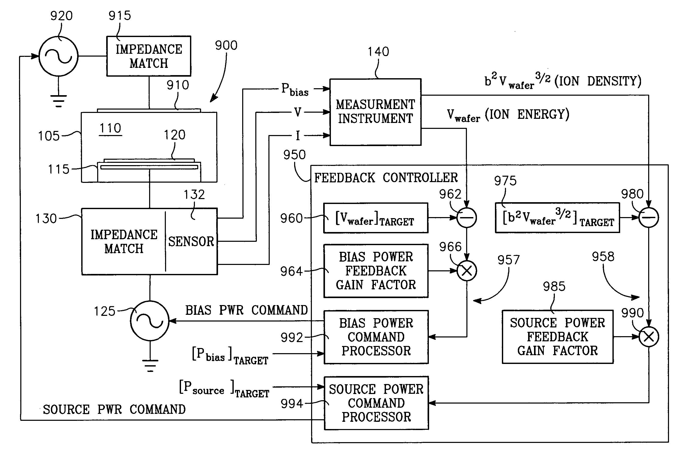
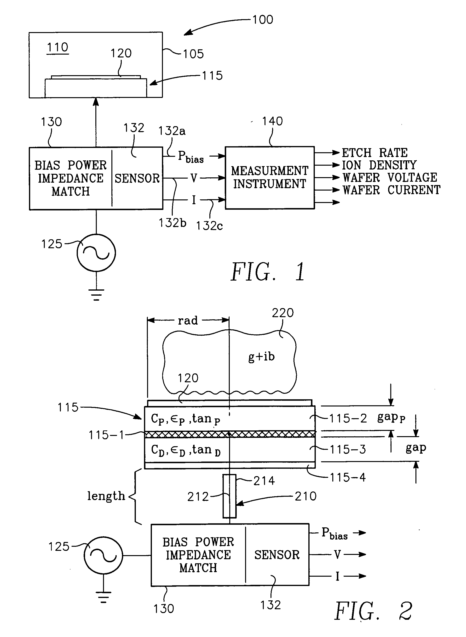
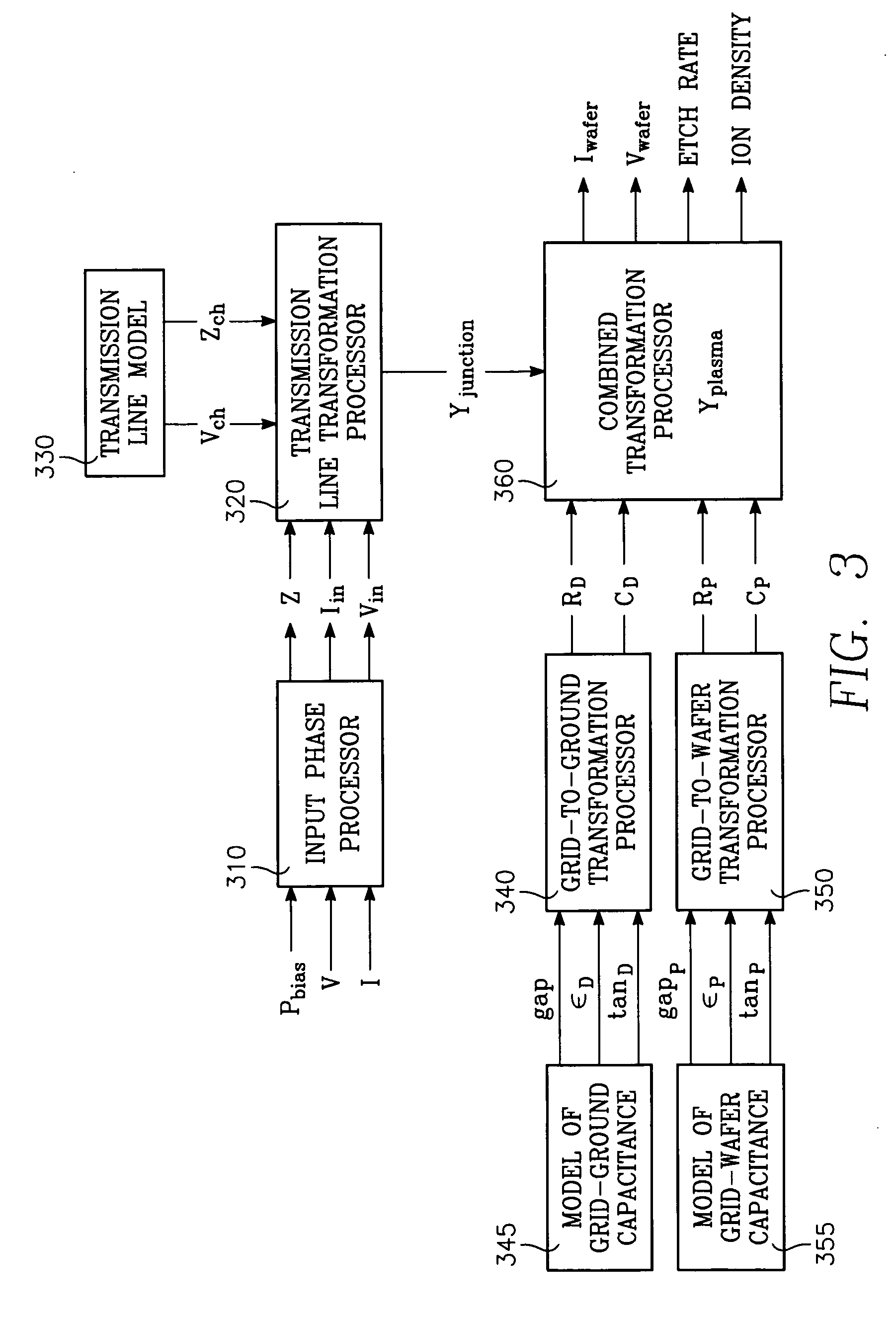
[0026] The present description pertains to a plasma reactor having a plasma source power applicator (such as an overhead electrode or antenna) in which plasma bias power is applied to the wafer through the wafer support pedestal. I have discovered a measurement instrument (described below) that is the first one known to instantaneously and accurately measure wafer voltage, wafer current, ion density and etch rate. The measurement instrument uses only conventional electrical sensors at the bias power input that sense voltage, current and power at the output of an impedance match device coupled to the wafer support pedestal. The measurement instrument is therefore non-invasive of the plasma etch process occurring within the reactor chamber in addition to being accurate. The degree of accuracy is surprising, surpassing even the best known instruments and measurement techniques currently in use.

[0027] I have invented a plasma reactor having a feedback controller employin...


PUM

PropertyMeasurementUnit
Lengthaaaaaaaaaa
Sizeaaaaaaaaaa
Densityaaaaaaaaaa

Abstract

Plasma parameters such as plasma ion density, wafer voltage, etch rate and wafer current in the chamber are determined from external measurements on the applied RF bias electrical parameters such as voltage and current. The method includes sensing RF parameters corresponding to an input impedance, an input current and an input voltage at the input of the impedance match element to a transmission line coupled between the bias generator and the wafer pedestal. The method continues by computing a junction admittance of a junction between the transmission line and the electrode within the wafer pedestal from the input impedance, input current and input voltage and from parameters of the transmission line. The method further includes providing shunt electrical quantities of a shunt capacitance between the electrode and a ground plane, and providing load electrical quantities of a load capacitance between the electrode and a wafer on the pedestal. The method further includes computing at least one of the plasma parameters from the junction admittance, the shunt electrical quantities, the load electrical quantities and a frequency of RF bias power applied to the electrode.

Description

CROSS-REFERENCE TO RELATED APPLICATIONS [0001] This application is a continuation of U.S. application Ser. No. 10 / 440,364, filed May 16, 2003 by Daniel Hoffman, entitled PLASMA DENSITY, ENERGY AND ETCH RATE MEASUREMENTS AT BIAS POWER INPUT AND REAL TIME FEEDBACK CONTROL OF PLASMA SOURCE AND BIAS POWER and assigned to the present assignee.BACKGROUND OF THE INVENTION [0002] Plasma reactors employed in microelectronic circuit fabrication can etch or deposit thin film layers on a semiconductor substrate. In a plasma reactive ion etch process, the etch rate, ion density, wafer voltage and wafer current are critical in controlling etch selectivity, wafer heating, etch striations, ion bombardment damage, etch stopping, feature size and other effects. Such control becomes more critical as feature size decreases and device density increases. The main problem is that present techniques for measuring etch rate, ion density, wafer voltage and wafer current tend to be highly inaccurate (in the c...

Claims


Application Information

Patent Timeline
IPC IPC(8): G01L21/30H01J37/32
CPCH01J37/32935H01J37/32174
Inventor HOFFMAN, DANIEL J.
Owner APPLIED MATERIALS INC
Why Eureka
Try Eureka