Stack circuit member and method

Inactive Publication Date: 2006-12-14
SAMSUNG ELECTRONICS CO LTD
View PDF5 Cites 22 Cited by
  • Summary
  • Abstract
  • Description
  • Claims
  • Application Information

AI Technical Summary

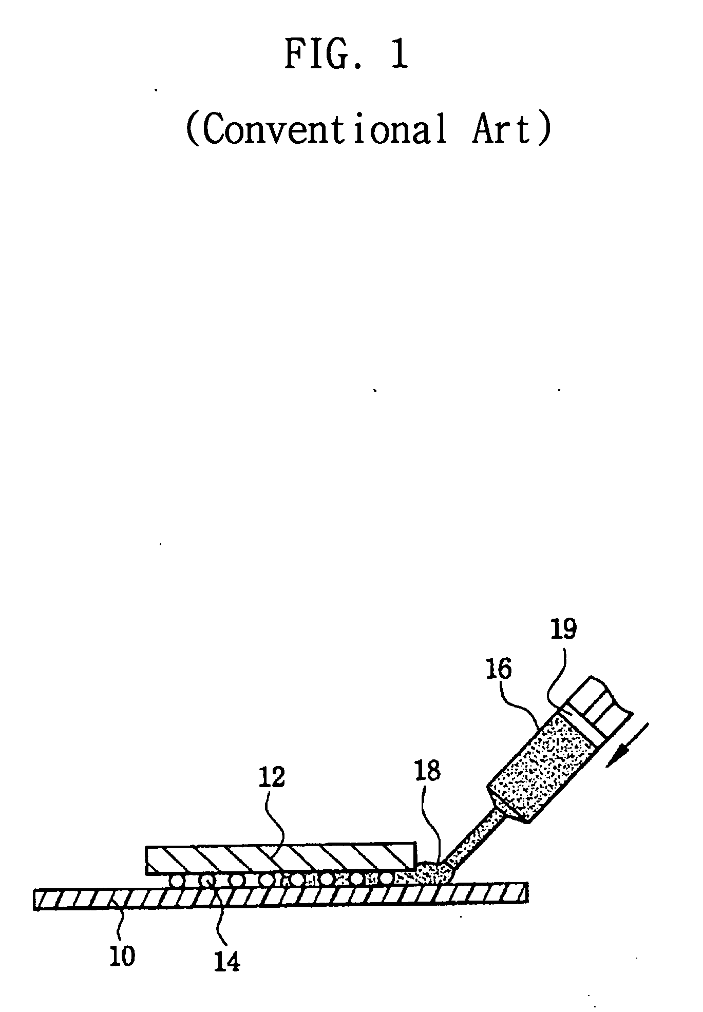
Problems solved by technology

Such faults may result from differences in coefficients of thermal expansion (CTEs) between the semiconductor chip and the wiring substrate, for example.
The dispensing method associated with the conventional gap fill process may have associated drawbacks.
If the gap fill process is performed at a wafer stage, the likelihood of voids may increase.
It may be time consuming to perform a gap fill process on a plura

Method used


Image

  • Stack circuit member and method
  • Stack circuit member and method
  • Stack circuit member and method

Examples


Embodiment Construction

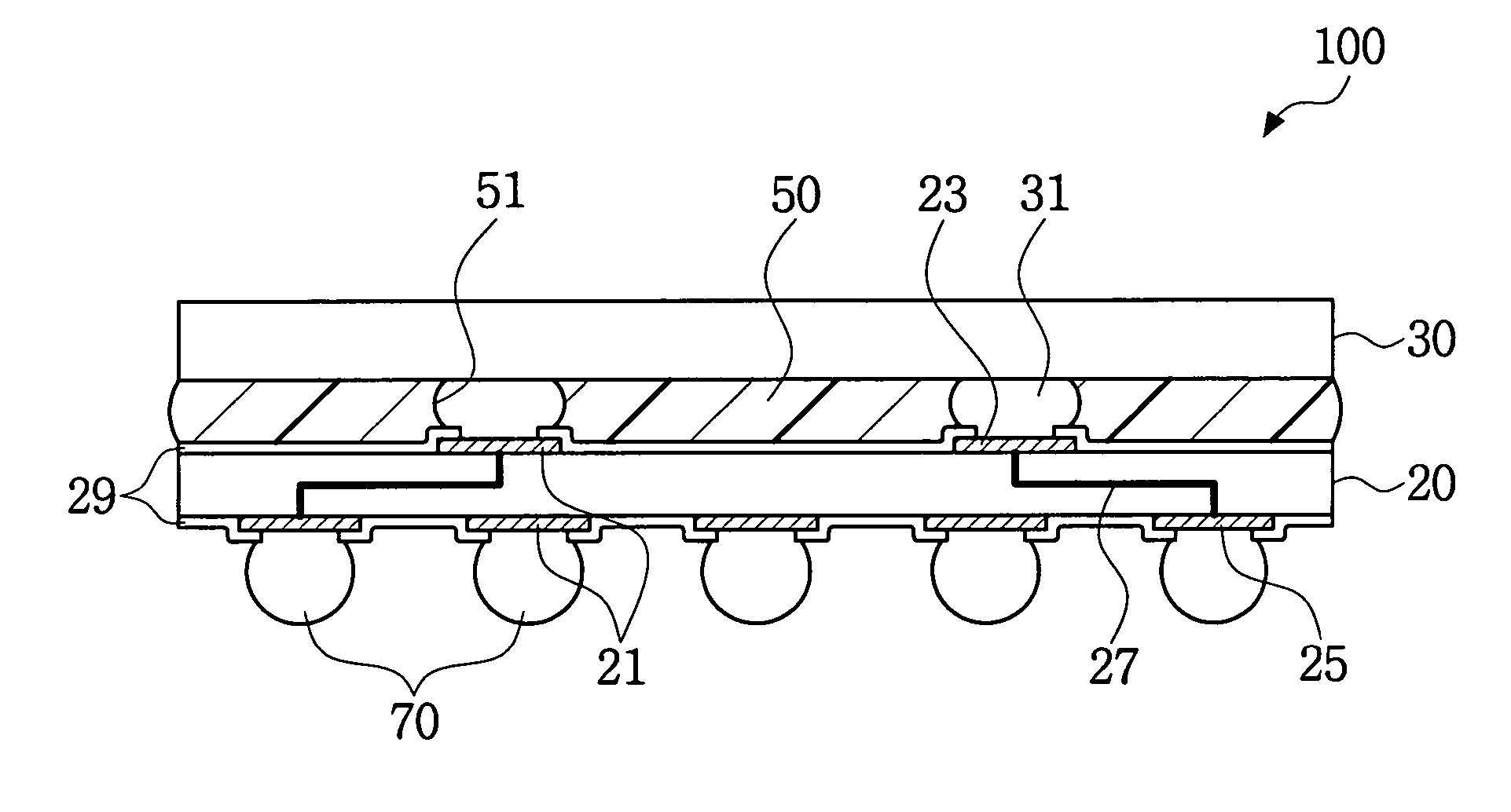
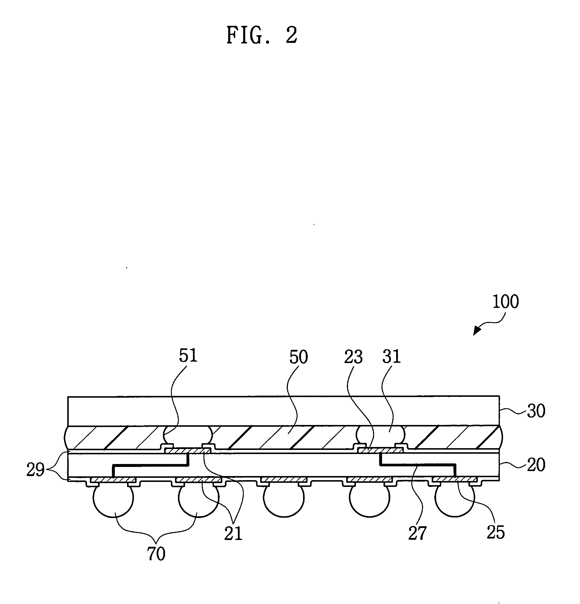
[0026] Example, non-limiting embodiments of the present invention will be described more fully with reference to the accompanying drawings. This invention may, however, be embodied in many different forms and should not be construed as limited to the example embodiments set forth herein. Rather, the disclosed embodiments are provided so that this disclosure will be thorough and complete, and will fully convey the scope of the invention to those skilled in the art. The principles and features of this invention may be employed in varied and numerous embodiments without departing from the scope of the invention.

[0027] An element is considered as being mounted (or provided) “on” another element when mounted or provided) either directly on the referenced element or mounted (or provided) on other elements overlaying the referenced element. Throughout this disclosure, spatial terms such as “upper,”“lower,”“above” and “below” (for example) are used for convenience in describing various ele...


PUM


Abstract

A stack circuit member may include a first circuit member and a second circuit member. The first and the second circuit members may be electrically and mechanically connected together using a thermocompression bonding method. A photosensitive polymer layer may be interposed between the first circuit member and the second circuit member. A gap fill process and an electrical connection process may be performed at the same time.

Description

PRIORITY STATEMENT [0001] This U.S. non-provisional application claims benefit of priority under 35 U.S.C. §119 from Korean Patent Application No. 2005-50501, filed on Jun. 13, 2005, the entire contents of which are incorporated herein by reference. BACKGROUND [0002] 1. Field of the Invention [0003] Example embodiments of the present invention relate in general to a stack circuit member and a method for manufacturing the stack circuit member, and more particularly, to a stack circuit member that may have a photosensitive polymer layer and a method for manufacturing the same. [0004] 2. Description of the Related Art [0005] Numerous and varied bonding techniques may be applied to semiconductor chips. Such techniques may include, for example, wire bonding, tape automated bonding (TAB), flip chip bonding, and anisotropic conductive film (ACF) bonding techniques. [0006] It may be desirable to develop methods, techniques and designs that may result in the manufacture of electronic product...

Claims


Application Information

Patent Timeline
IPC IPC(8): H01L23/52
CPCH01L21/563H01L21/6835H01L21/76898H01L23/481H01L24/81H01L25/0657H01L25/50H01L2221/6834H01L2221/68354H01L2224/16225H01L2224/16237H01L2224/73203H01L2224/73204H01L2224/81001H01L2224/81203H01L2224/81801H01L2224/83102H01L2224/83191H01L2224/83192H01L2224/83194H01L2224/83856H01L2224/92125H01L2225/06513H01L2225/06517H01L2225/06541H01L2924/01005H01L2924/01013H01L2924/01029H01L2924/01052H01L2924/01078H01L2924/01079H01L2924/12044H01L2924/14H01L2924/15174H01L2924/15311H01L2924/01006H01L2924/01033H01L2924/014H01L24/29H01L2224/32225H01L2924/0132H01L24/83H01L2224/16145H01L2224/73104H01L2224/81191H01L2224/32145H01L2924/00H01L2224/29011H01L2924/00011H01L2924/00014H01L2924/15787H01L2924/351H01L2224/0401H01L23/28H01L23/538
Inventor KWON, YONG-CHAILEE, KANG-WOOKMA, KEUM-HEEHAN, SEONG-II
Owner SAMSUNG ELECTRONICS CO LTD
Why Eureka
Try Eureka