Semiconductor device and method for fabricating the same

a technology of semiconductor devices and semiconductors, applied in the direction of semiconductor devices, electrical devices, transistors, etc., can solve the problems of increasing the gate leakage current caused by tunnel current coming to the surface, deteriorating carrier mobility, and inability to obtain desired operating current, so as to reduce the equivalent oxide thickness of the gate insulating film, prevent the increase of the absolute value of a threshold voltage, and reduce the effect of carrier mobility

Inactive Publication Date: 2006-12-14
INTERUNIVERSITAIR MICRO ELECTRONICS CENT (IMEC VZW)
View PDF3 Cites 5 Cited by
  • Summary
  • Abstract
  • Description
  • Claims
  • Application Information

AI Technical Summary

Benefits of technology

[0029] The first through third methods preferably further includes the step of performing nitridation on the gate insulating film, between the step of performing the heat treatment at a temperature at which the phases are stable and the step of forming the gate electrode. Then, a defect occurring in the gate insulating film made of a high-κ dielectric is compensated and, in addition, the equivalent oxide thickness of the gate insulating film is reduced.
[0030] With semiconductor devices and methods for fabricating the devices according to the present invention, in a transistor including a gate insulating film using a high-κ material, deterioration of carrier mobility and increase of the absolute value of a threshold voltage are prevented and thermodynamically stable characteristics are obtained.

Problems solved by technology

As the thickness of a gate insulating film decreases in accordance with this size reduction, the problem of increased gate leakage current caused by tunnel current comes to the surface.
In the initial stage of development, the use of a gate insulating film made of metal oxide such as HfO2 or ZrO2 causes a problem in which an interface layer is formed between a silicon substrate and the gate insulating film.
However, once the formation of an interface layer was successfully suppressed so that a high effective relative dielectric constant of the gate insulating film is maintained, i.e., the equivalent oxide thickness EOT is reduced afterward, there arises another problem in which carrier mobility deteriorates as compared to the case of a silicon oxide film and, consequently, desired operating current cannot be obtained.
It has been considered that a cause of this problem is that (1) fixed charge included in a high-κ material electrically interferes with carriers in channel to cause the carrier mobility to deteriorate or (2) carriers in channel are scattered by a lattice in the high-κ material to cause the carrier mobility to deteriorate, for example.
In addition, in recent yeas, there arises another problem in which the absolute value of the threshold voltage Vt during transistor operation increases due to reaction at the upper interface of the gate insulating film, i.e., reaction between materials for the gate insulating film and the gate electrode.
However, even these methods have a problem in which the dielectric constant of the buffer layer is lower than that of the high-κ material and the buffer layer is grown to be an island shape during deposition thereof so that the thickness needs to be large.
In addition, the silicate structure having a low metal concentration causes a problem in which the effective dielectric constant of the gate insulating film is extremely reduced (i.e., the equivalent oxide thickness EOT is increased) as described above.
However, these proposals have new problems dependent on a high-κ film deposition mechanism such as island-shape growth dependent on the underlying film as well as the buffer film and thermodynamic instability of the designed film structure.

Method used


Image

  • Semiconductor device and method for fabricating the same
  • Semiconductor device and method for fabricating the same
  • Semiconductor device and method for fabricating the same

Examples


embodiment 1

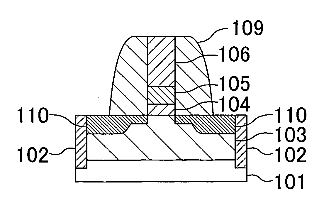
[0077] A semiconductor device according to a first embodiment of the present invention, which is a MOSFET including a gate insulating film made of high-κ metal oxide, will be described with reference to FIGS. 1 and 2.

[0078] First, as shown in FIG. 1, an nMOSFET according to the first embodiment is formed in a transistor region surrounded by an isolation film 102 serving as a shallow trench isolation (STI) and selectively formed in an upper portion of a substrate 101 made of silicon (Si) having a principal surface whose plane orientation is the (100) plane, for example.

[0079] In the transistor region, a well 103 having a junction depth approximately equal to the lower end of the isolation film 102 is formed. The well 103 is of a p-type when the MOSFET is an n-transistor and is of an n-type when the MOSFET is a p-transistor.

[0080] An underlying film 104 made of silicon oxide (SiO2) and having a thickness of about 0.5 nm, a gate insulating film 105 made of hafnium silicate (HfxSi1-x...

embodiment 2

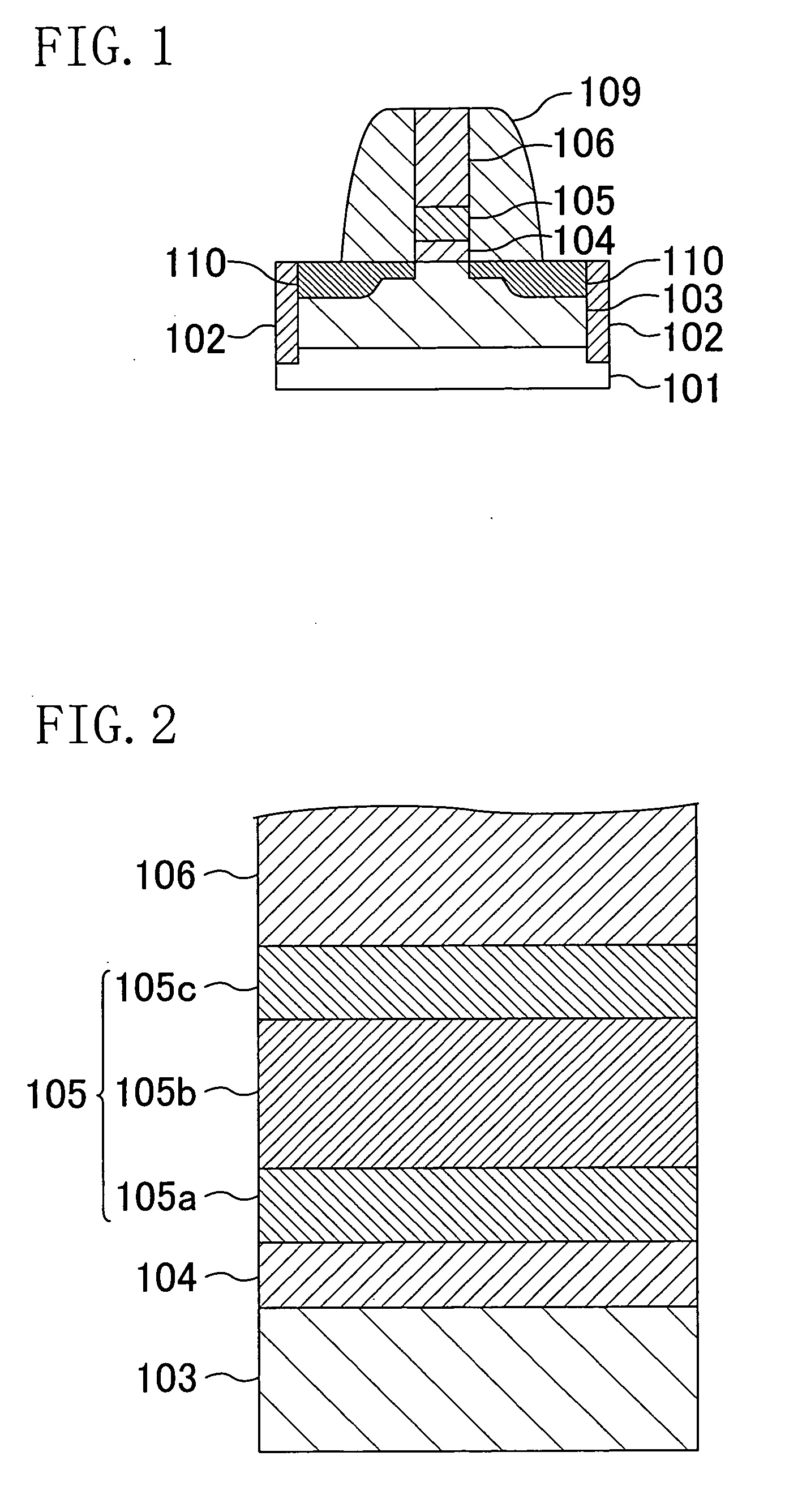
[0099] Hereinafter, a semiconductor device according to a second embodiment of the present invention, which is a MOSFET including a gate insulating film made of high-κ metal oxide, will be described with reference to FIGS. 5 and 6. In FIGS. 5 and 6, components also shown in FIG. 1 are denoted by the same reference numerals, and description thereof will be omitted.

[0100] In the second embodiment, as illustrated in an enlarged partial cross-sectional view of FIG. 6, a gate insulating film 205 made of high-κ metal oxide, i.e., hafnium silicate (HfxSi1-xO4), is composed of a first metal oxide film 205a of a low-κ stable phase having a Hf concentration x of 0.25 with a thickness of 1.0 nm, a second metal oxide film 205b of a high-κ stable phase having a Hf concentration x of 1 with a thickness of 1.5 nm, and a third metal oxide film 205c of a low-κ stable phase having a Hf concentration x of 0.25 with a thickness of 0.5 nm.

[0101] In the second embodiment, the gate insulating film 205 i...

embodiment 3

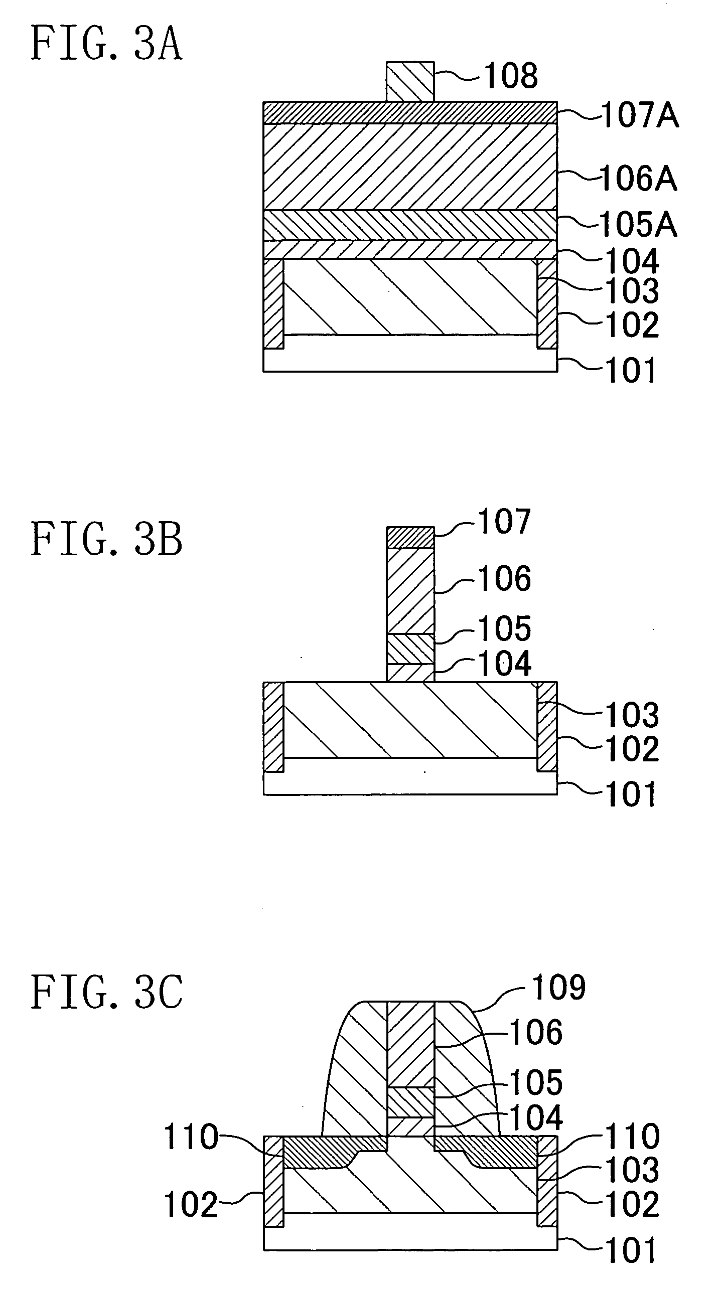
[0109] Hereinafter, a semiconductor device according to a third embodiment of the present invention, which is a MOSFET including a gate insulating film made of high-κ metal oxide, will be described with reference to FIGS. 7 and 8. In FIGS. 7 and 8, components also shown in FIG. 1 are denoted by the same reference numerals, and description thereof will be omitted.

[0110] In the third embodiment, as illustrated in an enlarged partial cross-sectional view of FIG. 8, a gate insulating film 305 made of high-κ metal oxide, i.e., hafnium silicate (HfxSi1-xO4) is composed of a first metal oxide film 305a of a low-κ stable phase having a Hf concentration x of 0.25 with a thickness of 1.0 nm, a second metal oxide film 305b of a high-κ stable phase having a Hf concentration x of 1 with a thickness of 1.5 nm, and a third metal oxide film 305c of a low-κ stable phase having a Hf concentration x of 0 with a thickness of 0.5 nm.

[0111] Now, a method for fabricating a MOSFET with the foregoing stru...


PUM


Abstract

A semiconductor device includes: a semiconductor substrate; a gate insulating film formed on the semiconductor substrate and made of a high-dielectric-constant material composed of a plurality of layers stacked perpendicularly to a principal surface of the semiconductor substrate and associated with respective phases; and a gate electrode formed on the gate insulating film.

Description

[0001] CROSS-REFERENCE TO RELATED APPLICATION [0002] The disclosure of Japanese Patent Application No. 2005-170210 filed on Jun. 9, 2005 including specification, drawings and claims is incorporated herein by reference in its entirety. BACKGROUND OF THE INVENTION [0003] The present invention relates to semiconductor devices, and particularly relates to a MOS device including a gate insulating film made of a dielectric material having a high dielectric constant (hereinafter, referred to as a high-κ material) and a method for fabricating the device. [0004] With recent increase in the integration degree and speed of semiconductor integrated circuit devices and expansion of the functionality thereof, the size of metal-oxide-semiconductor field effect transistors (MOSFETs) has been reduced. As the thickness of a gate insulating film decreases in accordance with this size reduction, the problem of increased gate leakage current caused by tunnel current comes to the surface. To solve this p...

Claims


Application Information

Patent Timeline
Patent Type & Authority Applications(United States)
IPC IPC(8): H01L21/336H01L29/76
CPCH01L21/28194H01L21/28229H01L21/823857H01L29/7833H01L29/517H01L29/6659H01L29/513
Inventor HAYASHI, SHIGENORIYAMAMOTO, KAZUHIKO
Owner INTERUNIVERSITAIR MICRO ELECTRONICS CENT (IMEC VZW)
Why Eureka
Try Eureka