Scavanging metal stack for a high-k gate dielectric

a high-k gate dielectric and metal stack technology, applied in the field of metal stack, can solve the problems of failure to achieve effective oxide thickness scaling, device leakage, and failure to provide high performance at or below the thickness of 1.1 nm, and achieve the effect of reducing the equivalent oxide thickness (eot) of the total gate dielectric and constant threshold voltag

Active Publication Date: 2010-12-23
GLOBALFOUNDRIES US INC
View PDF2 Cites 77 Cited by
  • Summary
  • Abstract
  • Description
  • Claims
  • Application Information

AI Technical Summary

Benefits of technology

[0004]The present invention provides a stack of a high-k gate dielectric and a metal gate structure includes a lower metal layer, a scavenging metal layer, and an upper metal layer. The scavenging metal layer meets the following two criteria 1) a metal (M) for which the Gibbs free energy change of the reaction Si+2 / y MxOy→2x / y M+SiO2 is positive 2) a metal that has a more negative Gibbs free energy per oxygen atom for formation of oxide than the material of the lower metal layer and the material of the upper metal layer. The scavenging metal layer meeting these criteria captures oxygen atoms as the oxygen atoms diffuse through the gate electrode toward the high-k gate dielectric. In addition, the scavenging metal layer remotely reduces the thickness of a silicon oxide interfacial layer underneath the high-k dielectric. As a result, the equivalent oxide thickness (EOT) of the total gate dielectric is reduced and the field effect transistor maintains a constant threshold voltage even after high temperature processes during CMOS integration.

Problems solved by technology

Scaling of the gate dielectric is a challenge in improving performance of advanced field effect transistors.
Such devices typically become too leaky to provide high performance at or below the thickness of 1.1 nm for the silicon oxide gate dielectric.
However, high-k gate dielectric materials are prone to a change in the effective oxide thickness (EOT) because high-k gate dielectric materials react with oxygen that diffuses through the gate electrode or gate spacers.
Regrowth of a silicon oxide interfacial layer between a silicon substrate and the high-k gate dielectric during high-temperature processing steps is a major obstacle to successful effective oxide thickness scaling.
Particularly, typical stacks of a high-k gate dielectric and a metal gate is known to be susceptible to a high temperature anneal in an oxygen ambient.
Such a high temperature anneal in oxygen ambient results in regrowth of the silicon oxide interfacial layer and produces instability of the threshold voltage of field effect transistors.

Method used


Image

  • Scavanging metal stack for a high-k gate dielectric
  • Scavanging metal stack for a high-k gate dielectric
  • Scavanging metal stack for a high-k gate dielectric

Examples


Embodiment Construction

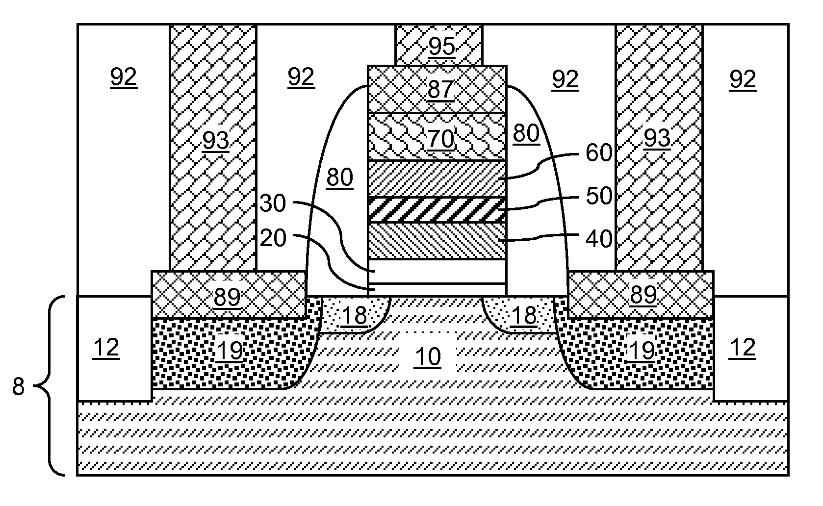
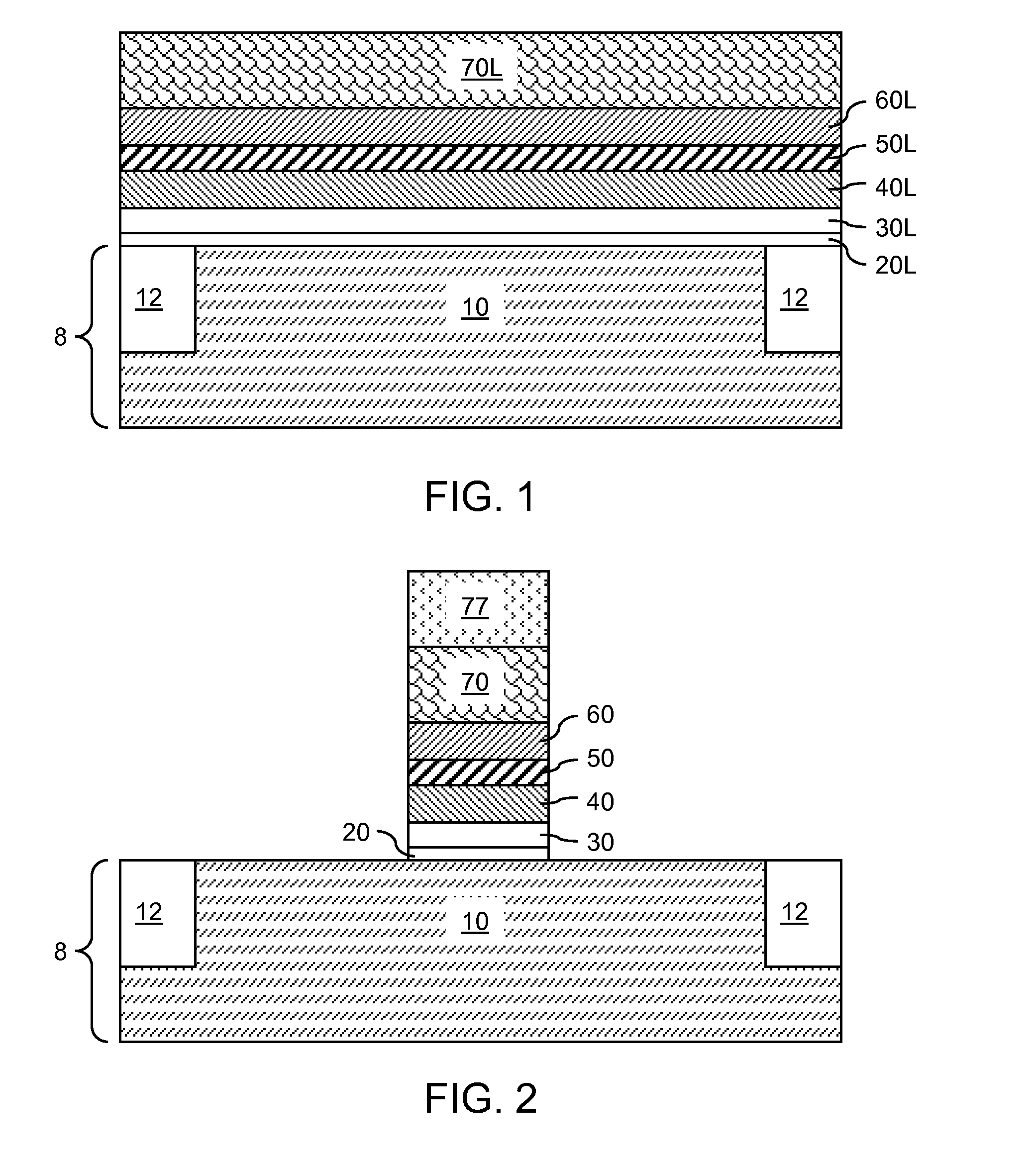
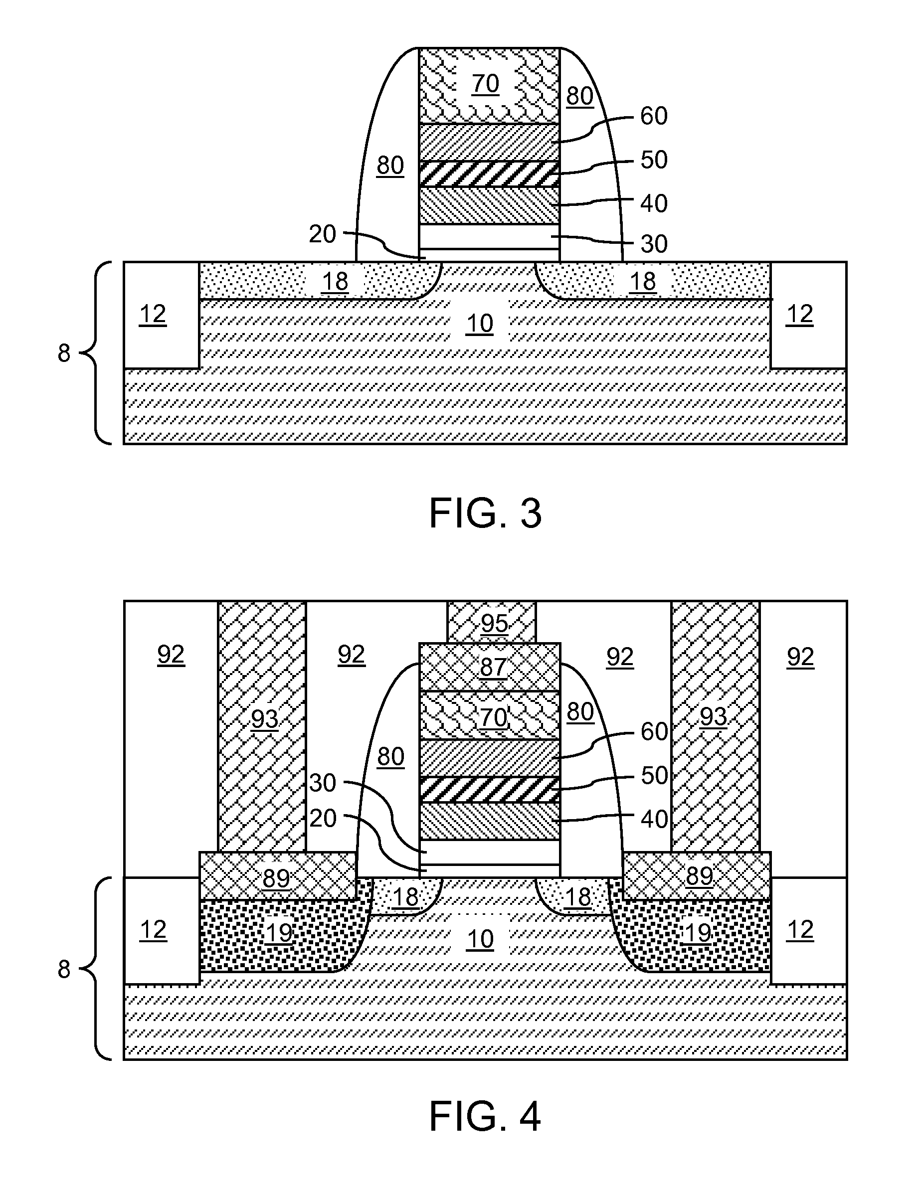
[0013]As stated above, the present invention relates to a metal gate stack included in an electrode over a high-k gate dielectric, and methods of manufacturing the same, which are now described in detail with accompanying figures. It is noted that like and corresponding elements are referred to by like reference numerals. The drawings are not drawn to scale.

[0014]Referring to FIG. 1, an exemplary semiconductor structure according to the present invention comprises a semiconductor substrate 8 and a stack of material layers formed thereupon. The semiconductor substrate 8 contains a substrate semiconductor layer 10 and shallow trench isolation structures 12. The substrate semiconductor layer 10 has a semiconductor material, which may be selected from, but is not limited to, silicon, germanium, silicon-germanium alloy, silicon carbon alloy, silicon-germanium-carbon alloy, gallium arsenide, indium arsenide, indium phosphide, III-V compound semiconductor materials, II-VI compound semicond...


PUM

PropertyMeasurementUnit
dielectric constantaaaaaaaaaa
thicknessaaaaaaaaaa
thicknessaaaaaaaaaa

Abstract

A stack of a high-k gate dielectric and a metal gate structure includes a lower metal layer, a scavenging metal layer, and an upper metal layer. The scavenging metal layer meets the following two criteria 1) a metal (M) for which the Gibbs free energy change of the reaction Si+2/y MxOy→2x/y M+SiO2 is positive 2) a metal that has a more negative Gibbs free energy per oxygen atom for formation of oxide than the material of the lower metal layer and the material of the upper metal layer. The scavenging metal layer meeting these criteria captures oxygen atoms as the oxygen atoms diffuse through the gate electrode toward the high-k gate dielectric. In addition, the scavenging metal layer remotely reduces the thickness of a silicon oxide interfacial layer underneath the high-k dielectric. As a result, the equivalent oxide thickness (EOT) of the total gate dielectric is reduced and the field effect transistor maintains a constant threshold voltage even after high temperature processes during CMOS integration.

Description

FIELD OF THE INVENTION[0001]The present invention generally relates to semiconductor devices, and particularly to a metal gate stack included in an electrode over a high-k gate dielectric, and methods of manufacturing the same.BACKGROUND[0002]Scaling of the gate dielectric is a challenge in improving performance of advanced field effect transistors. In a field effect transistor employing a silicon oxide based gate dielectric, the leakage current through the gate dielectric increases exponentially with the decrease in the thickness of the gate dielectric. Such devices typically become too leaky to provide high performance at or below the thickness of 1.1 nm for the silicon oxide gate dielectric.[0003]High-k gate dielectric provides a way of scaling down the thickness of the gate dielectric without an excessive increase in the gate leakage current. However, high-k gate dielectric materials are prone to a change in the effective oxide thickness (EOT) because high-k gate dielectric mate...

Claims


Application Information

Patent Timeline
Patent Type & Authority Applications(United States)
IPC IPC(8): H01L29/78H01L21/314H01L21/336
CPCH01L21/28088H01L29/4966H01L29/517H01L29/7833H01L29/665H01L29/6659H01L29/518H01L29/42312
Inventor ANDO, TAKASHICHOI, CHANGHWANFRANK, MARTIN M.NARAYANAN, VIJAY
Owner GLOBALFOUNDRIES US INC
Why Eureka
Try Eureka