Semiconductor device and a method of manufacturing the same
- Summary
- Abstract
- Description
- Claims
- Application Information
AI Technical Summary
Benefits of technology
Problems solved by technology
Method used
Image
Examples
first embodiment
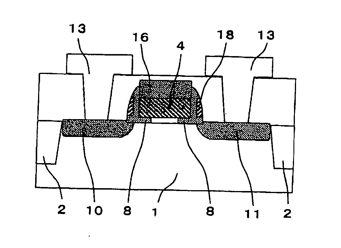
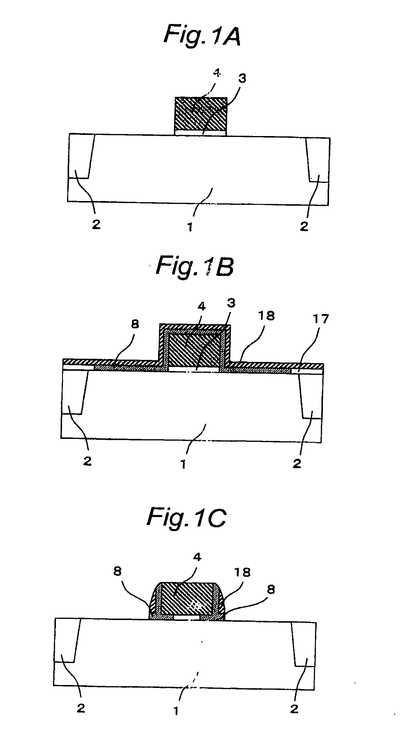
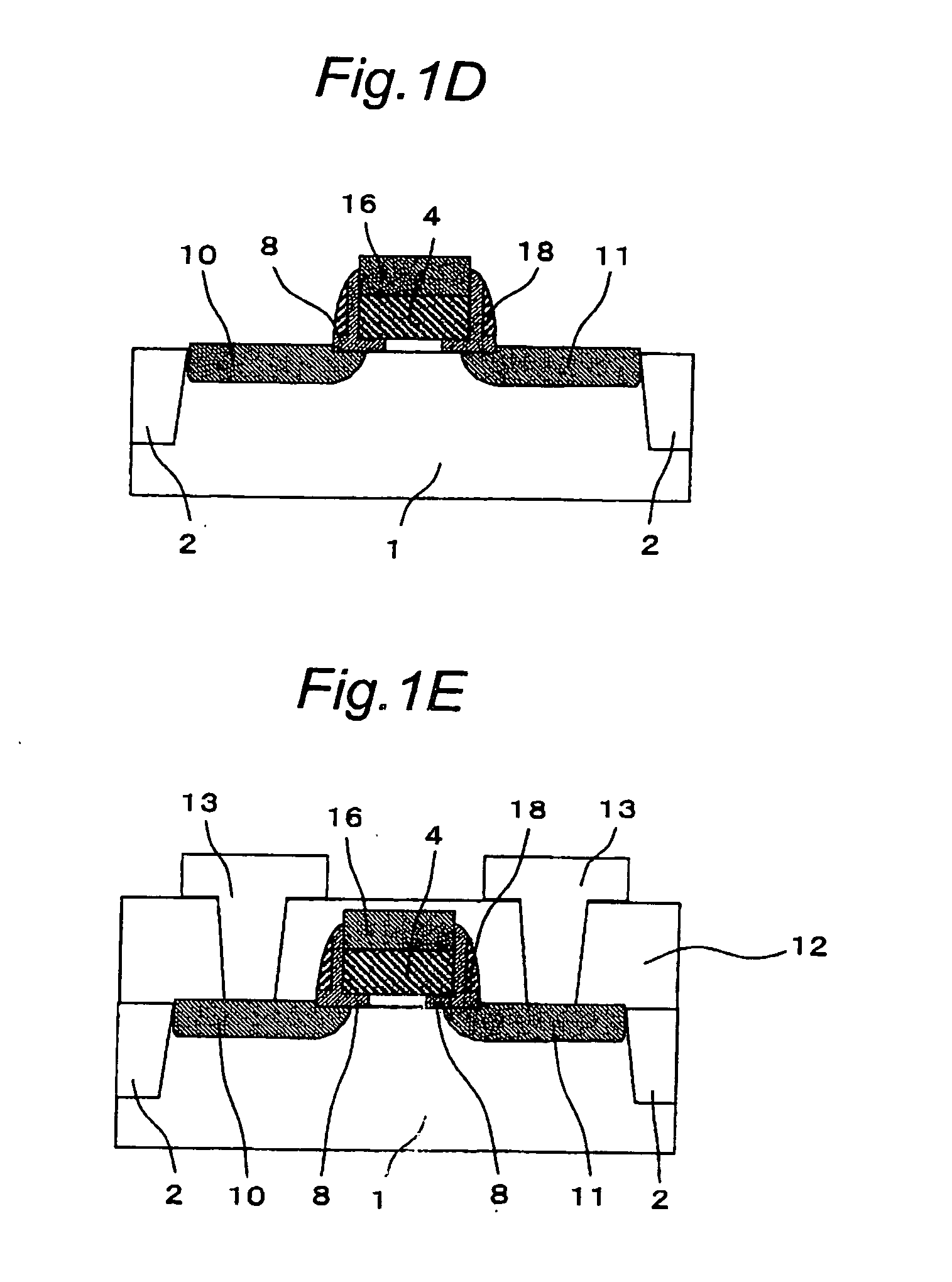
[0090] The semiconductor device of the first embodiment of the present invention is a Schottky-barrier-source / drain MIS field-effect transistor which is so structured that the source region and drain region made of metallic material overlap the gate electrode, wherein fixed charges are generated by doping cesium into an insulating film provided on a region of the substrate where the channel region is in contact with the source region and on a region of the substrate where the channel region is in contact with the drain region, thereby realizing the control of the threshold voltage as intended. That is, the semiconductor device of the first embodiment has a gate electrode, which is provided on the channel region of the semiconductor between the source region and the drain region, on a portion of the source region near the channel region, and on a portion of the drain region near the channel region, via a gate insulating film which has, at its end portions, regions containing fixed ch...
second embodiment
[0126] The semiconductor device of the second embodiment of the present invention is an n-type channel MIS field-effect transistor which has a source region and a drain region made of metallic material, and source and drain extensions consisting of inversion layers induced by fixed charge made of cesium, and which has been realized by simple processes. That is, the semiconductor device of the second embodiment has a gate electrode which is provided on the channel region of the semiconductor between the source region and the drain region via a gate insulating film, and both sides of the gate electrode are partially in contact with fixed-charge containing regions of an insulating layer. In this embodiment, the fixed-charge containing region extends from each of positions corresponding to two opposed side surfaces of the gate electrode to a position on each of the source and drain regions.
[0127]FIGS. 7A to 7E are cross-sectional views of the semiconductor device of the second embodime...
third embodiment
[0155] The semiconductor device of the third embodiment of the present invention is manufactured in such a way that the position of cesium to become fixed charges is deeper than the position of the interface between the gate insulating film and the silicon substrate. Because of this, the capacitance between the gate electrode and the fixed charges can be sufficiently less than the capacitance between the silicon substrate and the fixed charges, so that the electric lines of force extending from the fixed charges are restricted from terminating at the gate electrode 4, and thereby it becomes possible that the electric lines of force terminate at the silicon substrate efficiently. Thus, the heights and widths of the Schottky barriers are modulated effectively, and the carrier densities of the inversion layers formed with the fixed charge are increased, and thereby the parasitic resistance is reduced and a larger drive current is obtained.
[0156]FIGS. 10A to 10F are cross-sectional vie...
PUM
 Abstract
Description
Claims
Application Information
 - R&D
- Intellectual Property
- Life Sciences
- Materials
- Tech Scout
- Unparalleled Data Quality
- Higher Quality Content
- 60% Fewer Hallucinations
Browse by: Latest US Patents, China's latest patents, Technical Efficacy Thesaurus, Application Domain, Technology Topic, Popular Technical Reports.
© 2025 PatSnap. All rights reserved.Legal|Privacy policy|Modern Slavery Act Transparency Statement|Sitemap|About US| Contact US: help@patsnap.com


