Thermal processing equipment calibration method

a technology of thermal processing equipment and calibration method, which is applied in the direction of heat measurement, semiconductor/solid-state device testing/measurement, instruments, etc., can solve the problems of inability to achieve direct calibration of thermal processing equipment, inapplicability to multi-layer type substrates, and the need for expensive soi wafers to be scrapped, so as to achieve easy operation, reduce slip lines, and reduce the effect of wafer deformation

Active Publication Date: 2006-12-21
S O I TEC SILICON ON INSULATOR THECHNOLOGIES
View PDF14 Cites 8 Cited by
  • Summary
  • Abstract
  • Description
  • Claims
  • Application Information

AI Technical Summary

Benefits of technology

[0014] Once the golden profile is established for a given multilayer substrate, the test substrate can be used anytime a new calibration of thermal processing equipment needs to be carried out. In fact, to calibrate a thermal processing equipment, it is now sufficient to form a layer on a new test substrate, to measure the layer thickness profile produced, and to compare it with the corresponding golden profile. If profile differences are observed, the process parameters can then be amended such that the differences are taken into account. When the amended set of thermal process parameters produces a thickness profile on the test substrate corresponding to the golden profile, the amended set of thermal process parameters will also produce a corresponding multilayer substrate. If the golden profile corresponds to a multilayer substrat...

Problems solved by technology

Such a direct calibration of thermal processing equipment is, however, not applicable to multilayer type substrates, for example, silicon on insulator (SOI) wafers.
This method does, however, have the problem that the calibration is not achieved in a direct way and that in fact a correlation between the heat absorption coefficients and the equipment parameters needs to be established.
This method, although being a direct way of calibrating, has nevertheless the drawback that...

Method used


Image

  • Thermal processing equipment calibration method
  • Thermal processing equipment calibration method
  • Thermal processing equipment calibration method

Examples


Embodiment Construction

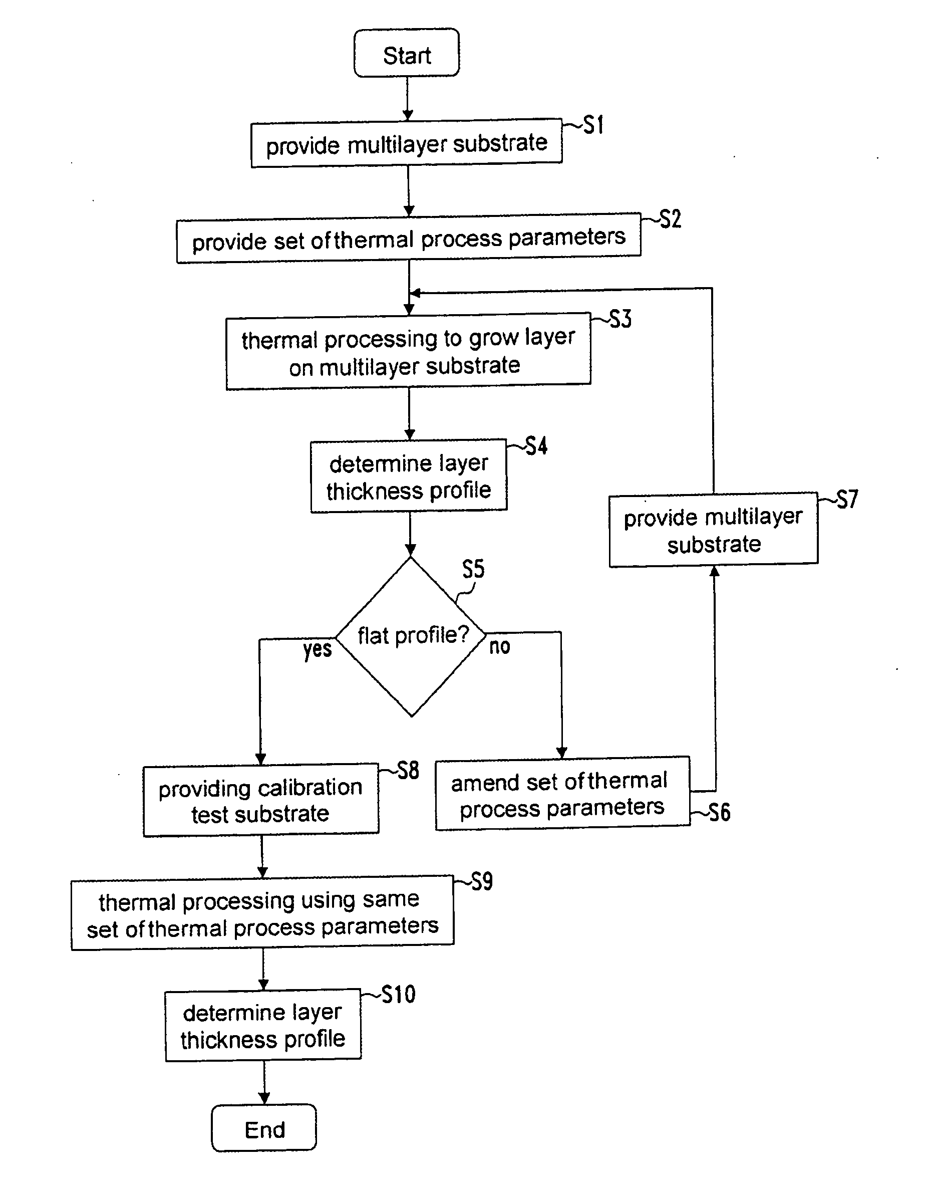
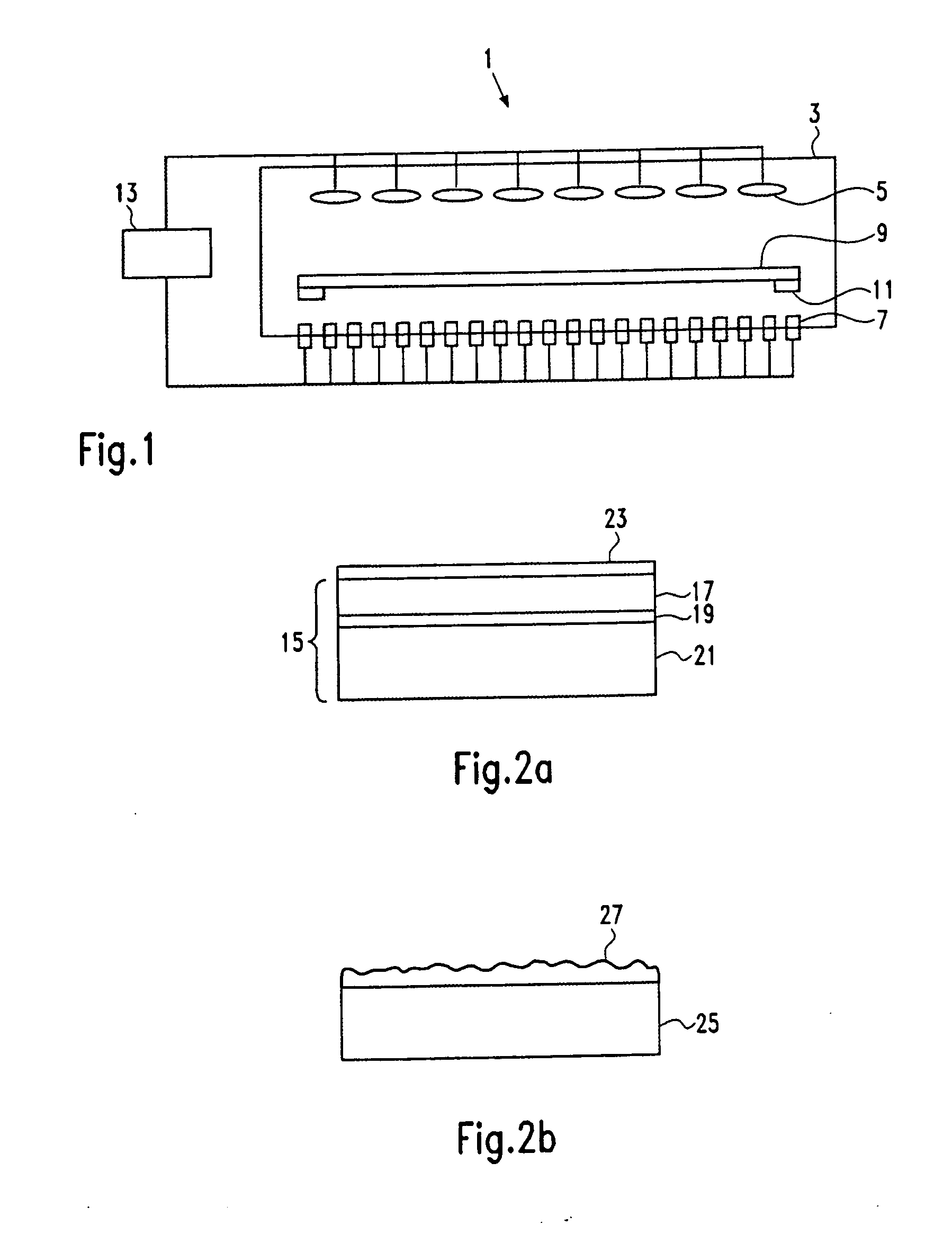
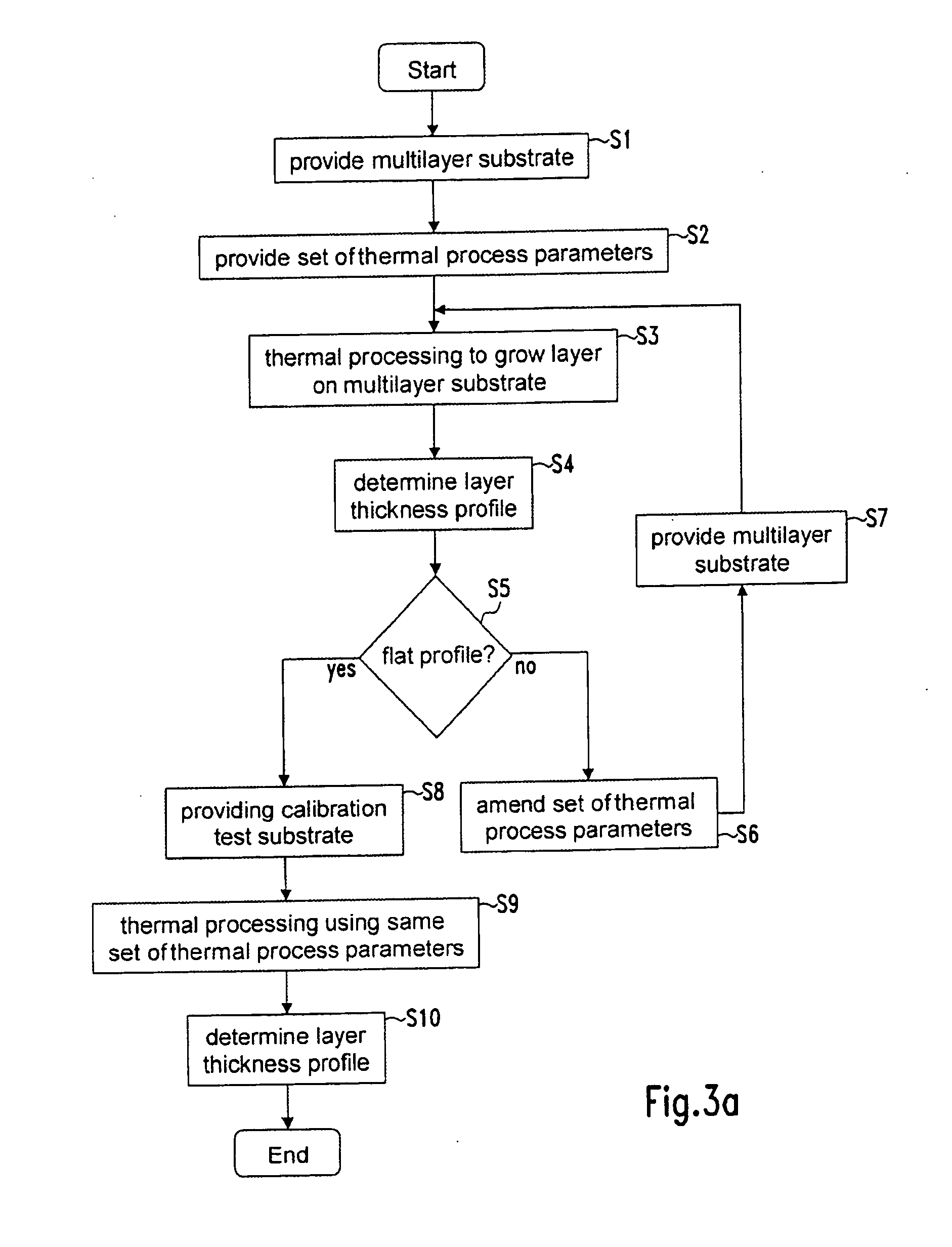
[0025] The terms “test substrates” and “calibration test substrates” refer to substrates with the same structure, except that a calibration test substrate is a test substrate that has been used for calibrating a heating device. During calibration of a heating device, the predetermined thickness profile (golden profile) of the calibration layer is formed on the calibration test substrate using the same thermal process parameters which, when used for processing multilayer substrates, produces multilayer substrates with an even thickness profile, or alternatively a multilayer substrate with reduced, in particular nearly no or no, slip lines and / or reduced wafer deformations. The term “thermal process parameters” relates to any controllable parameter of the equipment that influences the heat profile in the equipment.

[0026] According to a preferred embodiment, the set of thermal process parameters used to process a test substrate correspond to a set of predetermined thermal process para...


PUM


Abstract

The invention relates to a method for calibrating thermal processing equipment used for heat treatment of a multilayer substrate, in particular a multilayer semiconductor substrate. A calibration test profile is determined by processing a calibration test substrate according to thermal process parameters that produce multilayer substrates having an even thickness profile, and/or having reduced slip lines and/or reduced wafer deformation, and/or having other desired and predetermined properties. Then a particular thermal processing equipment is calibrated by determining thermal process parameters for that equipment so that a test substrate processed with these parameters will have the determined calibration test profile.

Description

FIELD OF THE INVENTION [0001] This invention relates to a method for calibrating thermal processing equipment comprising a heating device which is used for heat treatment of a multilayer substrate, in particular a semiconductor multilayer substrate. The invention furthermore relates to a calibration test substrate and a method for creating the calibration test substrate. BACKGROUND [0002] Thermal processing equipment is usually used for thermally treating semiconductor wafers in a hydrogen, argon or oxygen atmosphere, in order to, for example, form an oxide layer or to smooth the surface of a wafer. In order to achieve uniform temperature across the wafers, the equipment needs to be calibrated. For this purpose temperature sensors (or probes) are positioned below the wafer which is usually positioned horizontally in a furnace chamber. These sensors measure the local temperature of the wafer and are connected to a control system which causes the equipment to adapt locally the amount ...

Claims


Application Information

Patent Timeline
IPC IPC(8): H01H71/16
CPCH01L22/12H01L22/20H01L2924/0002H01L2924/00H01L21/324
Inventor BRAS, MARLENE
Owner S O I TEC SILICON ON INSULATOR THECHNOLOGIES
Why Eureka
Try Eureka