Low work function metal alloy

a low work function, metal alloy technology, applied in the direction of semiconductor devices, electrical apparatus, transistors, etc., can solve the problems of not being able to teach the formation of a fully silicided gate electrode using such binary alloys, unable to achieve the desired work function of both nmos and pmos devices in view of controlling the threshold voltage, and the threshold voltage is too high compared with the supply voltage, etc., to achieve the effect of easy implementation

Inactive Publication Date: 2006-12-21
INTERUNIVERSITAIR MICRO ELECTRONICS CENT (IMEC VZW) +1
View PDF10 Cites 42 Cited by
  • Summary
  • Abstract
  • Description
  • Claims
  • Application Information

AI Technical Summary

Benefits of technology

[0010] The preferred embodiments aim at providing a new low work function material, which is stable, reprodu...

Problems solved by technology

However, obtaining the desired work function for both nMOS and pMOS devices in view of controlling the threshold voltage is not as straightforward as in the case of polysilicon gates, as the work function of polysilicon can be tuned by doping the polysilicon with a well-defined amount of an appropriate dopant, e.g., boron for pMOS devices, thereby forming a high work function gate electrode, and ...

Method used


Image

  • Low work function metal alloy
  • Low work function metal alloy
  • Low work function metal alloy

Examples


example

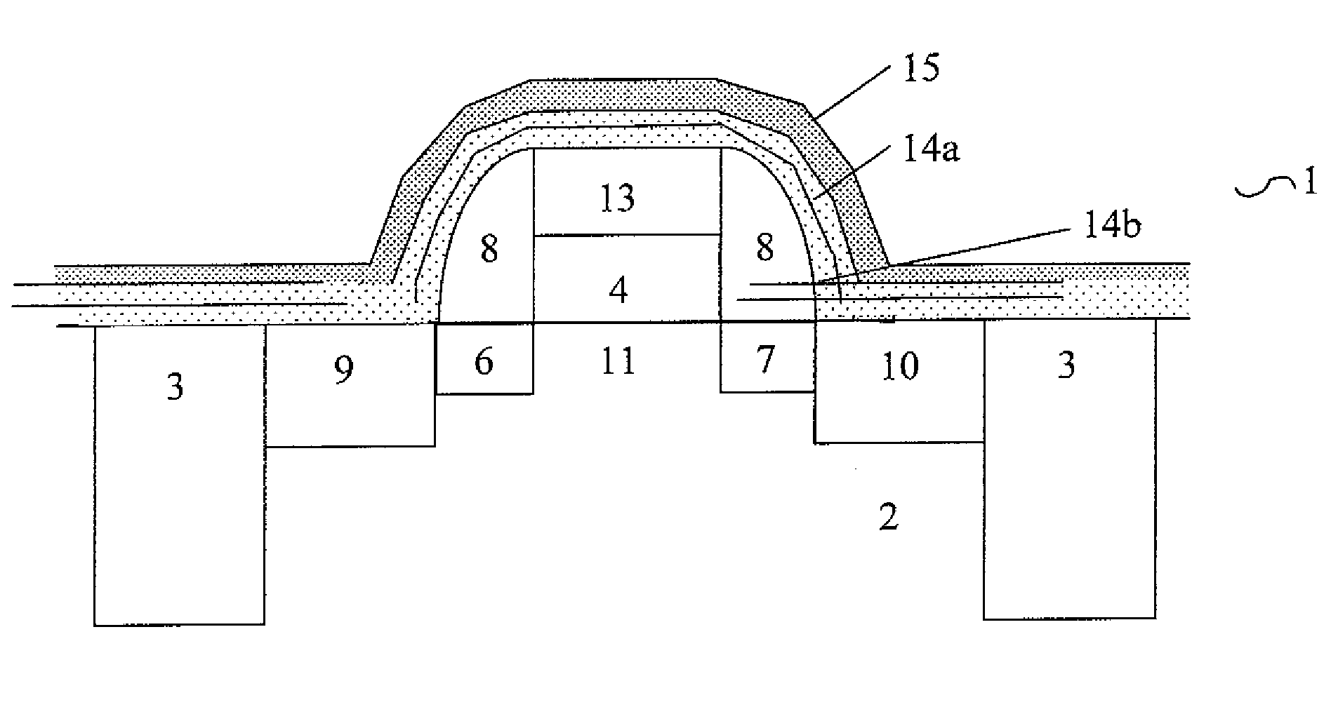
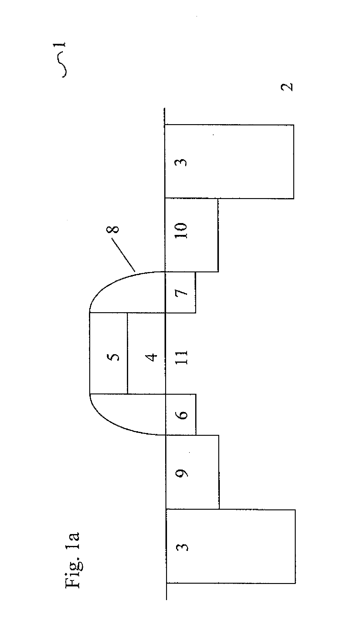
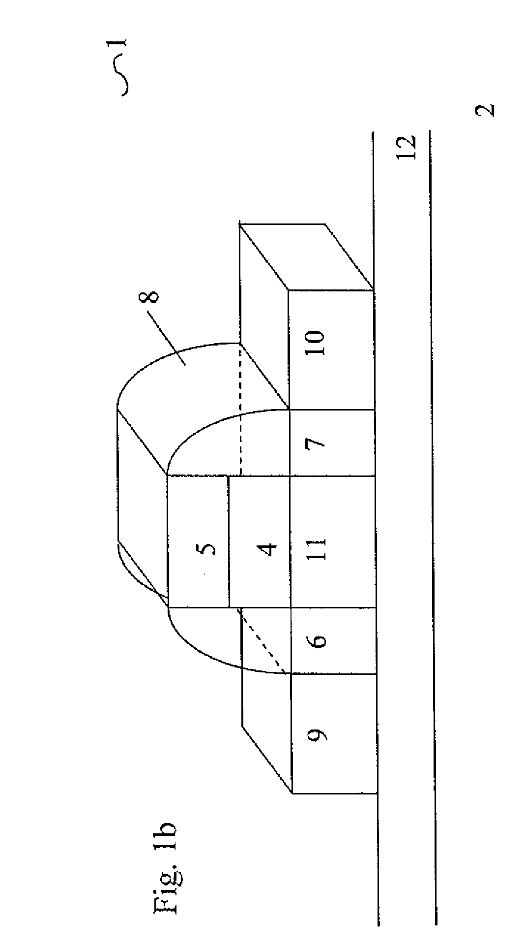
[0200] In an embodiment as depicted in FIG. 2f, the formation of a NiYb silicide is disclosed.

[0201] On p-type silicon substrates (2) MOS capacitors were fabricated by first depositing a SION dielectric layer (4) thereon.

[0202] SiON layers with various thicknesses have been formed on various wafers.

[0203] On top of each dielectric layer (4) undoped polysilicon (13) is deposited using Chemical Vapor Deposition (CVD).

[0204] The polysilicon layer (13) had a thickness of about 100 nm. On top of each polysilicon layer a layer stack (14) of ytterbium (Yb) (14a) and nickel (Ni) (14b) was deposited by Plasma Vapor Depositing (VPD) in an argon ambient. Yb was deposited at a rate of about 10 nm / min, and Ni at a rate of about 17 nm / min.

[0205] Firstly both Ni and Yb were co-sputtered for 1.5 min. Then the deposition of Yb was stopped while the deposition of Ni was continued for another 2.5 min.

[0206] In total about 68 nm of Ni and about 15 nm of Yb was deposited resulting in a total metal...


PUM


Abstract

Low work function metals for use as gate electrode in nMOS devices are provided. The low work function metals include alloys of lanthanide(s), metal and semiconductor. In particular, an alloy of nickel-ytterbium (NiYb) is used to fully silicide (FUSI) a silicon gate. The resulting nickel-ytterbium-silicon gate electrode has a work function of about 4.22 eV.

Description

CROSS-REFERENCE TO RELATED APPLICATIONS [0001] This application claims the benefit under 35 U.S.C. § 119(e) of U.S. provisional application Ser. No. 60 / 680,276, filed May 11, 2005, the disclosure of which is hereby incorporated by reference in its entirety and is hereby made a portion of this application.FIELD OF THE INVENTION [0002] The present invention relates to the field of semiconductor devices, in particular to field effect devices comprising a metal gate electrode, more particularly a metal gate electrode formed by silicidation of a semiconductor material and to methods for fabricating such field effect devices. BACKGROUND OF THE INVENTION [0003] In order to improve the performance of MOSFET devices the well known polysilicon is being replaced as gate electrode material by metals. Such metal gates do not suffer from the shortcomings of a semiconducting gate electrode such as gate depletion, dopant diffusion or medium range resistance. However, obtaining the desired work func...

Claims


Application Information

Patent Timeline
IPC IPC(8): H01L21/44
CPCH01L21/265H01L21/28088H01L21/28097H01L21/28518H01L29/785H01L21/823864H01L29/665H01L29/6659H01L21/823842
Inventor YU, HONGYUJINGDE, CHENMINGFU, LIKWONG, DIM-LEEBIESEMANS, SERGEKITTL, JORGE ADRIAN
Owner INTERUNIVERSITAIR MICRO ELECTRONICS CENT (IMEC VZW)
Why Eureka
Try Eureka