

Scanning photolithography apparatus and method
a photolithography and scanning technology, applied in the field of scanning photolithography apparatus and method, can solve the problems of reducing the yield of the semiconductor device being fabricated, and achieve the effect of reducing the overall exposure time and increasing productivity
- Summary
- Abstract
- Description
- Claims
- Application Information
AI Technical Summary
Benefits of technology
Problems solved by technology
Method used
Image

Examples
Embodiment Construction
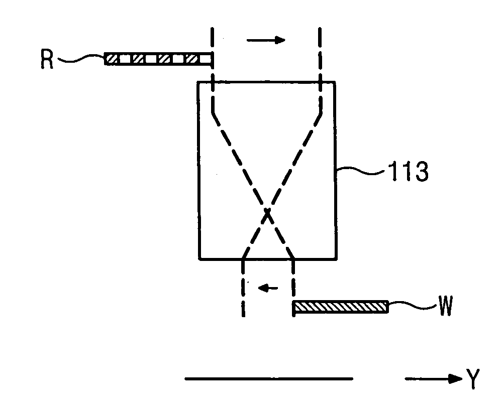
[0028] Several embodiments of the invention will now be described with reference to the accompanying drawings. While the invention is described in the context of these embodiments, those of ordinary skill in the art will recognize that the invention may be variously embodied and that the illustrated embodiments are presented as teaching examples. Thus, invention should not be construed as being limited to only the exemplary embodiments set forth herein. Throughout the description like reference numerals refer to like or similar elements.
[0029] In the description of exemplary embodiments that follows, a wafer (e.g., a silicon wafer) is assumed to be the subject substrate. However, other substrate types may be used instead of a conventional wafer. For example, a wafer formed from semiconductor material may be used for a glass plate such as those adapted for use in planar display devices (e.g., LCD, FED and PDP type devices).
[0030] The term “enlargement ratio” used throughout refers ...
PUM
 Abstract
Description
Claims
Application Information