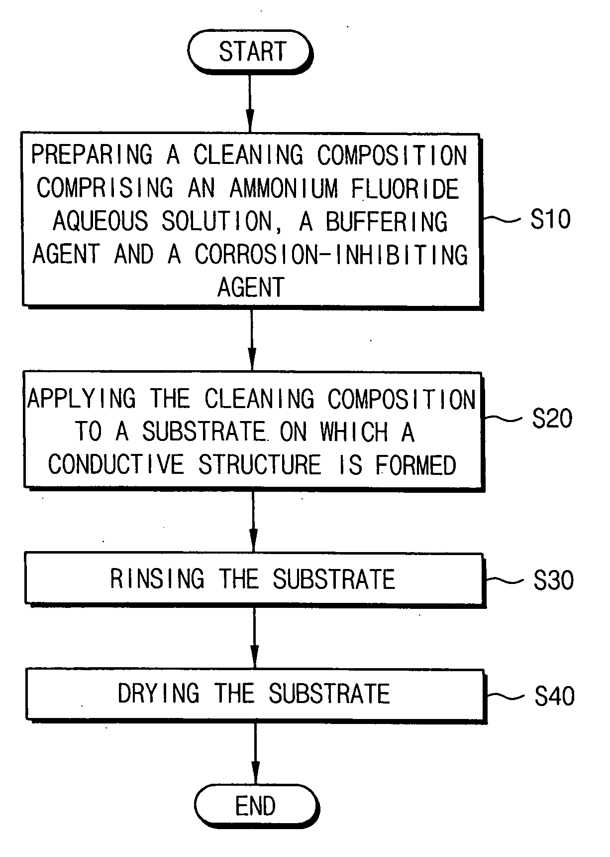
Cleaning composition and related methods
a technology of cleaning composition and composition, applied in the field of cleaning composition, can solve the problems of reducing the reliability of a semiconductor device produced through that process, the productivity of a semiconductor manufacturing process, and the inability of conventional cleaning solutions to clean a substrate, etc., to reduce the damage to a conductive structure, and the amount of contamination of the conductive structure.
- Summary
- Abstract
- Description
- Claims
- Application Information
AI Technical Summary
Benefits of technology
Problems solved by technology
Method used
Image

Examples
example 1
[0131] A cleaning composition was prepared using about 1 percent by weight of tetramethylammonium hydroxide, about 0.1 percent by weight of hydrogen fluoride, about 1.2 percent by weight of a buffering agent, about 0.001 percent by weight of a corrosion-inhibiting agent, and a remainder of pure water, based on the total weight of the cleaning composition. Ammonium nitrate was used as the buffering agent, and an anionic surfactant was used as the corrosion-inhibiting agent. NCW-1002 (trade name; manufactured by Wako Co., Japan) was used as the anionic surfactant. In preparing the cleaning composition, an ammonium fluoride aqueous solution was prepared by mixing tetramethylammonium hydroxide (TMAH), hydrogen fluoride, and pure water; and then the buffering agent and the corrosion-inhibiting agent were added to the ammonium fluoride aqueous solution. The cleaning composition thus prepared had a pH of about 10.5.
examples 2 through 7
[0132] Cleaning compositions were prepared by processes substantially the same as those described with reference to Example 1 except for the amount (i.e., content) of hydrogen fluoride, and the type and amount of the corrosion-inhibiting agent in the cleaning compositions of Examples 2 through 7. The types and amounts of the components in and the pH levels of the cleaning compositions prepared in Examples 1 through 7 are shown in Table 1.
PUM
 Abstract
Description
Claims
Application Information
 - R&D
- Intellectual Property
- Life Sciences
- Materials
- Tech Scout
- Unparalleled Data Quality
- Higher Quality Content
- 60% Fewer Hallucinations
Browse by: Latest US Patents, China's latest patents, Technical Efficacy Thesaurus, Application Domain, Technology Topic, Popular Technical Reports.
© 2025 PatSnap. All rights reserved.Legal|Privacy policy|Modern Slavery Act Transparency Statement|Sitemap|About US| Contact US: help@patsnap.com