
Methods of Fabricating Crystalline Silicon Film and Thin Film Transistors

a technology of crystalline silicon film and thin film transistor, which is applied in the direction of semiconductor devices, basic electric elements, electrical equipment, etc., can solve the problems of non-uniform tft characteristics, high cost of ela process, long-term oled operation difficulty, etc., and achieves reduced thermal budget, reduced thermal budget, and reduced thermal budget

Active Publication Date: 2007-01-04
KAKKAD RAMESH
View PDF8 Cites 13 Cited by
  • Summary
  • Abstract
  • Description
  • Claims
  • Application Information

AI Technical Summary

Benefits of technology

[0014] The invention presents a method by which solid phase crystallization (SPC) thermal budget for crystallizing an undoped (or a lightly doped) amorphous Si (a-Si) is significantly reduced. First, a composite layer structure consisting of an undoped (or a lightly doped) a-Si layer and a heavily doped (either p-type or n-type) a-Si layer is formed and it is subsequently annealed at an elevated temperature. The solid phase crystallization starts from the heavily doped amorphous silicon layer at a substantially reduced thermal budget and proceeds to crystallize the undoped amorphous silicon film in contact with the heavily doped film at reduced thermal budget. The method can be applied to form poly silicon thin film transistor at reduced thermal budgets.

Problems solved by technology

For OLED applications, currently the use of polysilicon TFTs is the only practical way to make reliable displays as instability of a-Si TFTs make long-term OLED operations difficult.
First of all, the ELA process is expensive in terms of cost of equipment, its operation and maintenance.
Secondly, since the ELA is performed by scanning a pulsed laser beam, there is a non-uniformity in TFT characteristics resulting from pulse-to-pulse variation of energy of the laser beam.
The high value of surface roughness for polysilicon formed by ELA process affects the TFT performance adversely.
However, the thermal budgets needed to crystallize a-Si by SPC are too high to be practical for mass production of TFTs.
Such times are too long for mass production of devices.
However, the glass substrate used for these TFTs can easily bend at these thermal budgets.
However, such higher-temperature-deposited a-Si films tend to have pre-existing crystal embryos, which result in higher nucleation density upon annealing, leading to reduced polysilicon grain-size.
The reduced Si grain-size lowers the device performance.
This method is very attractive because of its lower thermal budget, but during the annealing, there is an incorporation of the metals or their silicides into the entire silicon layer, which affect the device characteristics adversely, especially the leakage current, which increases significantly for these devices.
Although the heavily doped silicon films can be crystallized in shorter times, they can not be used as channels in TFTs.

Method used


Image

  • Methods of Fabricating Crystalline Silicon Film and Thin Film Transistors
  • Methods of Fabricating Crystalline Silicon Film and Thin Film Transistors
  • Methods of Fabricating Crystalline Silicon Film and Thin Film Transistors

Examples


Embodiment Construction

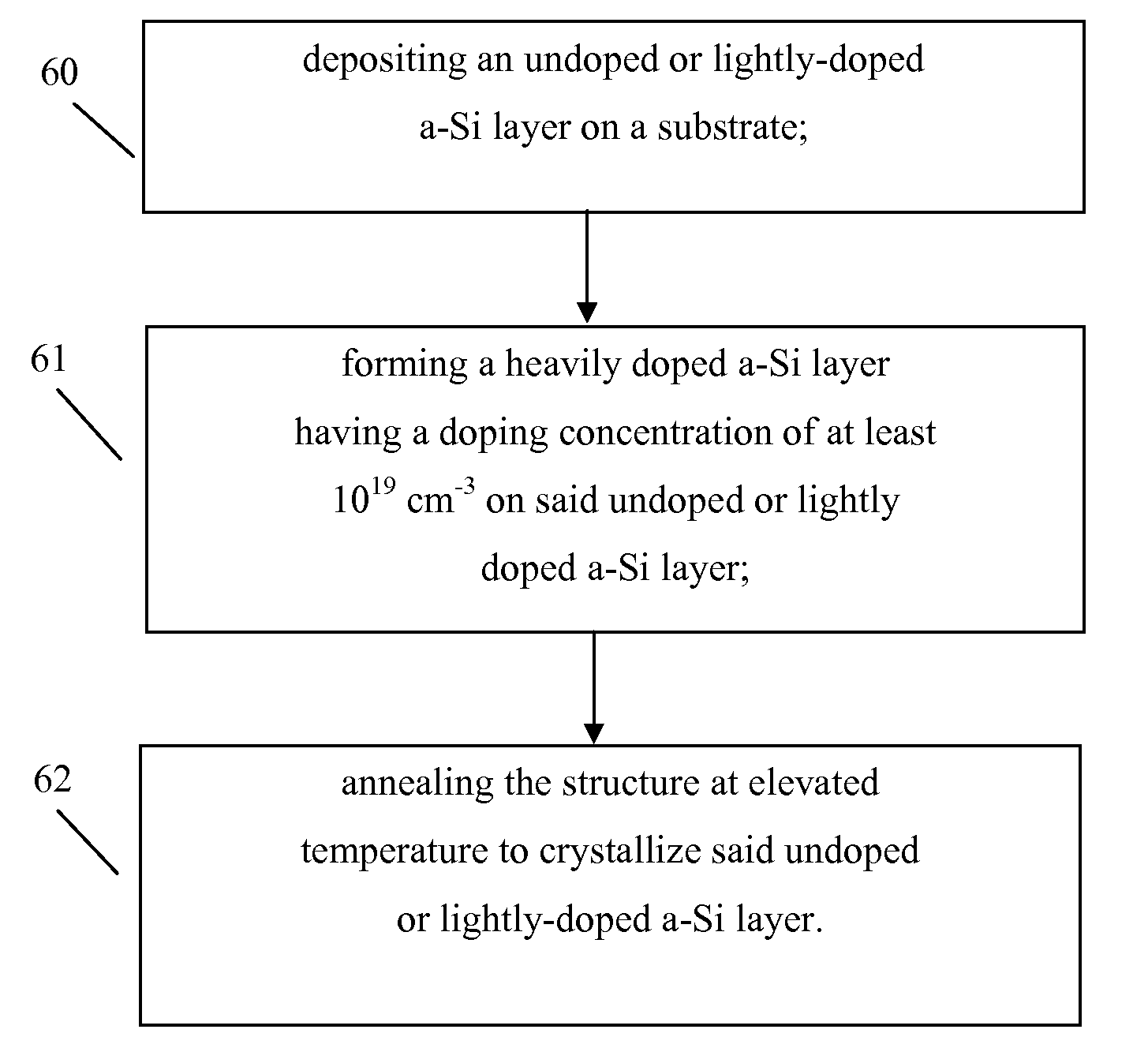
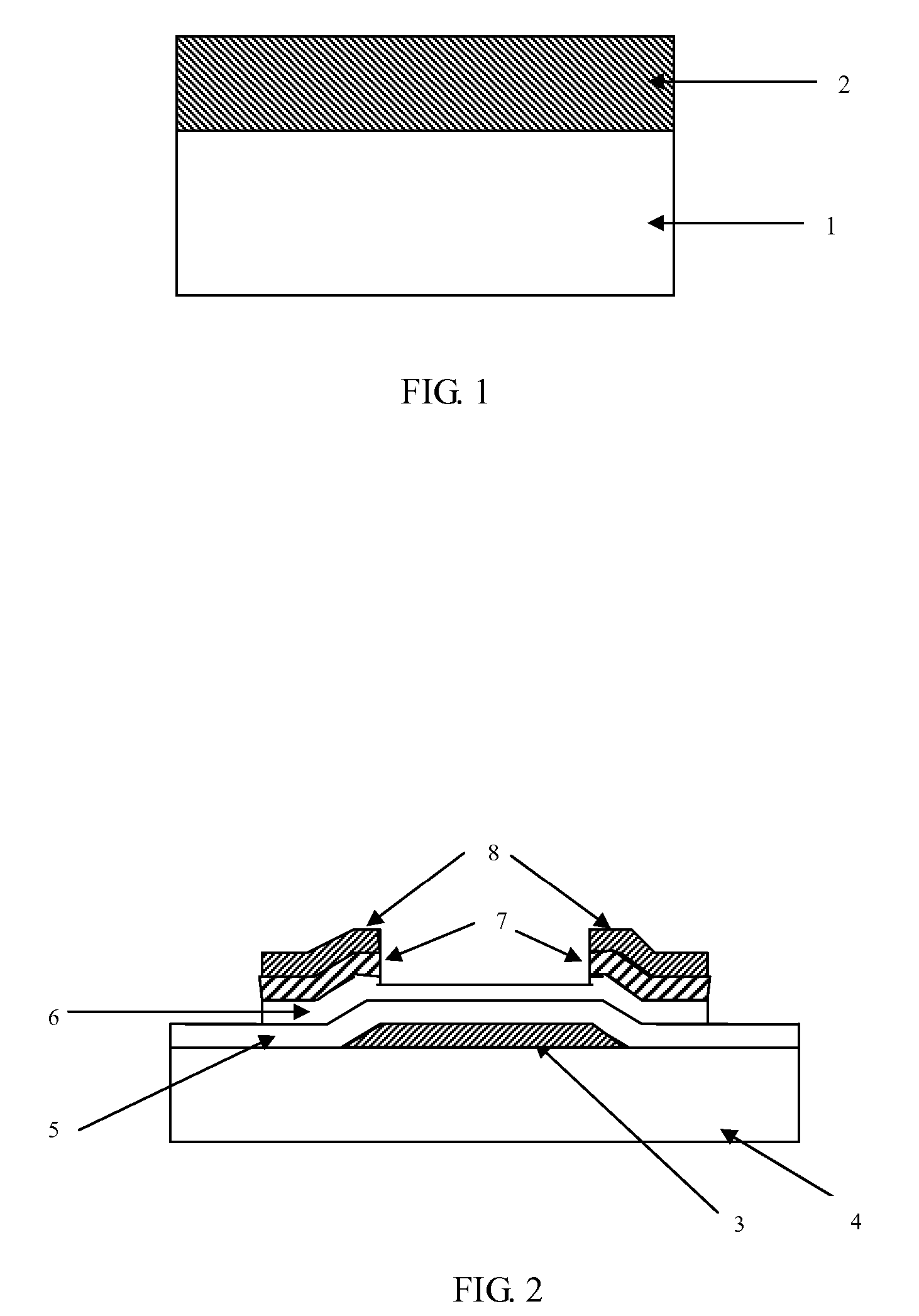
[0021]FIG. 6 shows a flowchart of the invention, as it might be used to create the structure shown schematically in FIG. 1. According to the method of the invention, step 60, an undoped a-Si film 1 (for example to be used as an active layer of TFT) of the desired thickness is deposited on a desired substrate. If needed, the undoped film can be lightly doped, for example, for threshold voltage adjustment of TFT, but the doping levels for this film would be very low (generally of the order of 1017 cm−3), so this film will be referred as undoped film. On this undoped a-Si film, step 61, a heavily gas-phase doped a-Si film 2 (for example boron doped film with doping concentrations in the range of 1020-1021 cm−3) is deposited without breaking the vacuum. The structure is then, step 62, annealed at an elevated temperature. The doped film 2 crystallizes at lower thermal budget as was mentioned earlier and crystallization process continues to the undoped layer.

[0022] The reduction in the c...


PUM


Abstract

A method by which solid phase crystallization (SPC) thermal budget for crystallizing an undoped (or a lightly doped) amorphous Si (a-Si) is significantly reduced. First, a composite layer structure consisting of an undoped (or a lightly doped) a-Si layer and a heavily doped (either p-type or n-type) a-Si layer is formed and it is subsequently annealed at an elevated temperature. The solid phase crystallization starts from the heavily doped amorphous silicon layer at a substantially reduced thermal budget and proceeds to crystallize the undoped amorphous silicon layer in contact with the heavily doped film at reduced thermal budget. The method can be applied to form poly silicon thin film transistor at reduced thermal budgets.

Description

REFERENCE TO RELATED APPLICATIONS [0001] This application claims an invention which was disclosed in Provisional Application No. 60 / 695,287, filed Jun. 30, 2005, entitled “Methods of Fabricating Crystalline Silicon Film and Thin Film Transistors”. The benefit under 35 USC §119(e) of the United States provisional application is hereby claimed, and the aforementioned application is hereby incorporated herein by reference.BACKGROUND OF THE INVENTION [0002] 1. Field of the Invention [0003] The invention pertains to the field of semiconductor fabrication. More particularly, the invention pertains to methods of crystallizing amorphous silicon film and methods of forming thin film transistor structures incorporating the silicon film formed using solid phase crystallization. [0004] 2. Description of Related Art [0005] Polycrystalline silicon (polysilicon) thin film transistor (TFT) arrays are used as backplanes for switching liquid crystal displays (LCDs) and also for driving organic light ...

Claims


Application Information

Patent Timeline
IPC IPC(8): H01L21/20H01L21/36
CPCH01L21/02532H01L21/02573H01L21/0262H01L29/66765H01L27/1281H01L27/1296H01L21/02672
Inventor KAKKAD, RAMESH
Owner KAKKAD RAMESH
Learn More