A Method and Apparatus for Reducing Leakage in Integrated Circuits

Active Publication Date: 2007-01-11
UNIV OF SOUTH FLORIDA
View PDF4 Cites 19 Cited by
  • Summary
  • Abstract
  • Description
  • Claims
  • Application Information

AI Technical Summary

Benefits of technology

[0029] As such, the method and apparatus for leakage control in CMOS circuits, in accordance with the present invention provides an efficient leakage power reduction method for deep submicron and nanometer circuits that is input v

Problems solved by technology

In deep submicron and nanometer CMOS circuits, the reduction of the threshold voltage due to voltag

Method used


Image

  • A Method and Apparatus for Reducing Leakage in Integrated Circuits
  • A Method and Apparatus for Reducing Leakage in Integrated Circuits
  • A Method and Apparatus for Reducing Leakage in Integrated Circuits

Examples


Example

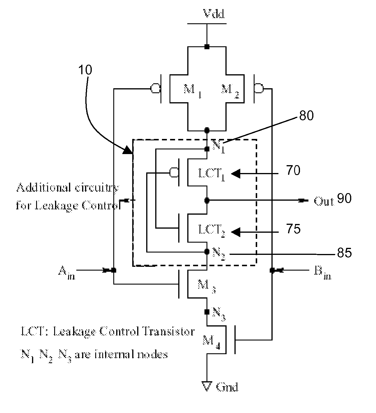
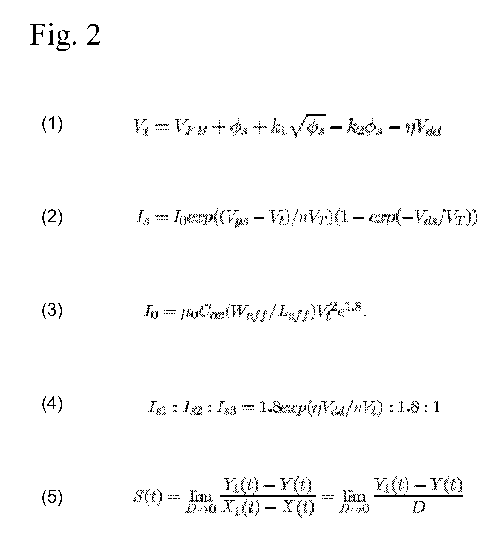
[0049] For short channel MOSFETs, the leakage current calculation is not straightforward due to the highly nonlinear behavior of the drain current of the device with respect to source / drain voltages. The present invention uses the Berkeley Short-Channel IGFET (BSIM) Predictive Technology Model to estimate the leakage power dissipation, as it fits well with HSPICE simulations. In the BSIM model, the threshold voltage (Vt)is expressed as in FIG. 2 (1), where VFB is the flat-band voltage, φs is twice the Fermi potential, k1 and k2 represent the non-uniform doping effect and η models the drain induced barrier lowering (DIBL) effect, an undesirable punch through / current flowing between the source and drain below the surface of the channel. The leakage current for NMOS transistors operating in weak-inversion region (i.e.=0) is given by FIG. 2 (2), where VT is the thermal voltage and is given by q / kT, n is the sub-threshold slope coefficient, and I0 is given by equation (3) of FIG. 3. As s...


PUM


Abstract

An efficient design methodology in accordance with the present invention is described for reducing the leakage power in CMOS circuits. The method and apparatus in accordance with the present invention yields better leakage reduction as the threshold voltage decreases and hence aids in further reduction of supply voltage and minimization of transistor sizes. Unlike other leakage control techniques, the technique of the present invention does not need any control circuitry to monitor the states of the circuit. Hence, avoiding the sacrifice of obtained leakage power reduction in the form of dynamic power consumed by the additional circuitry to control the overall circuit states.

Description

BACKGROUND OF INVENTION [0001] One of the most popular Metal-Oxide-Semiconductor Field Effect Transistor (MOSFET) technologies available today is the complementary MOS (metal oxide semiconductor), or CMOS, technology. This technology makes use of both P and N channel devices in the same substrate material. Such devices are extremely useful, since the same signal that turns on a transistor of one type is used to turn off a transistor of the other type. A MOSFET transistor consists of three regions, referred to as the “source”, the “gate” and the “drain”. In an N-type transistor, the source and drain regions are doped with N type material and the substrate doped with P type material. In a P-type transistor, the source and drain regions are doped with P type material, and the substrate is doped with N type material. The source and drain regions are quite similar, and are labeled depending on to what they are connected. The source is the terminal, or node, which acts as the source of ch...

Claims


Application Information

Patent Timeline
IPC IPC(8): H03K19/003H01L
CPCH03K17/162H03K17/6872H03K2217/0036H03K19/00361H03K19/0013
Inventor RANGANATHAN, NAGARAJANHANCHATE, NARENDER
Owner UNIV OF SOUTH FLORIDA
Why Eureka
Try Eureka