Ferroelectric storage device
a storage device and ferroelectric technology, applied in the field of ferroelectric storage devices, can solve the problems of insufficient constraint of a variation of a characteristic, and achieve the effect of stable detection
- Summary
- Abstract
- Description
- Claims
- Application Information
AI Technical Summary
Benefits of technology
Problems solved by technology
Method used
Image
Examples
first embodiment
[0028] A first embodiment of the invention will hereinafter be explained with reference to the drawings in FIGS. 1 through 7 and FIGS. 11 through 14.
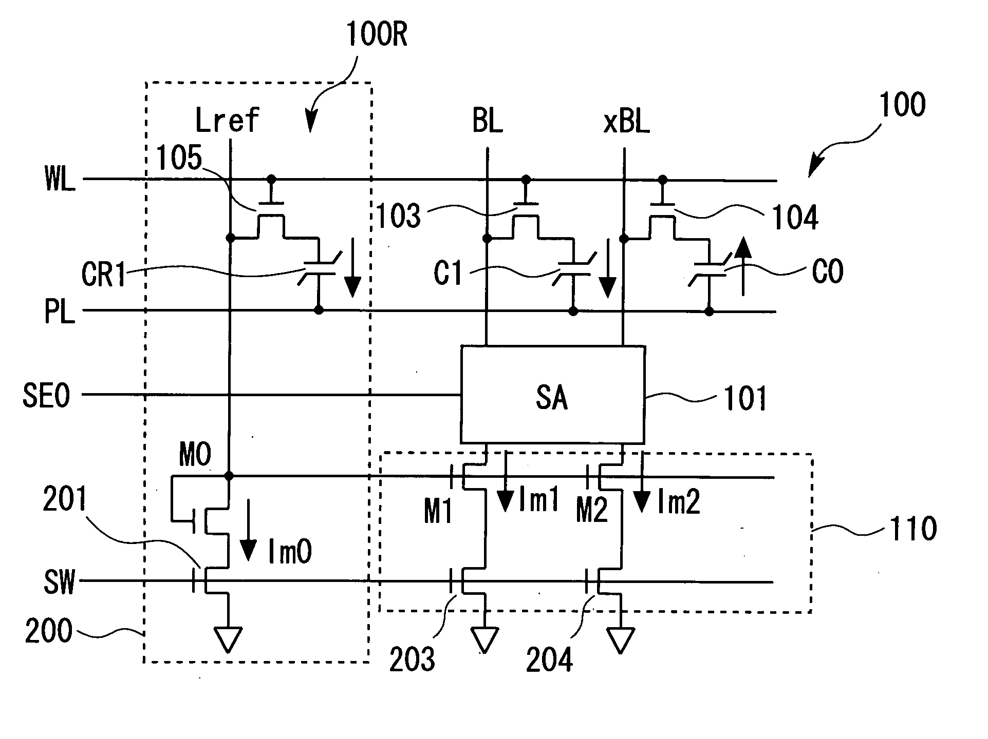
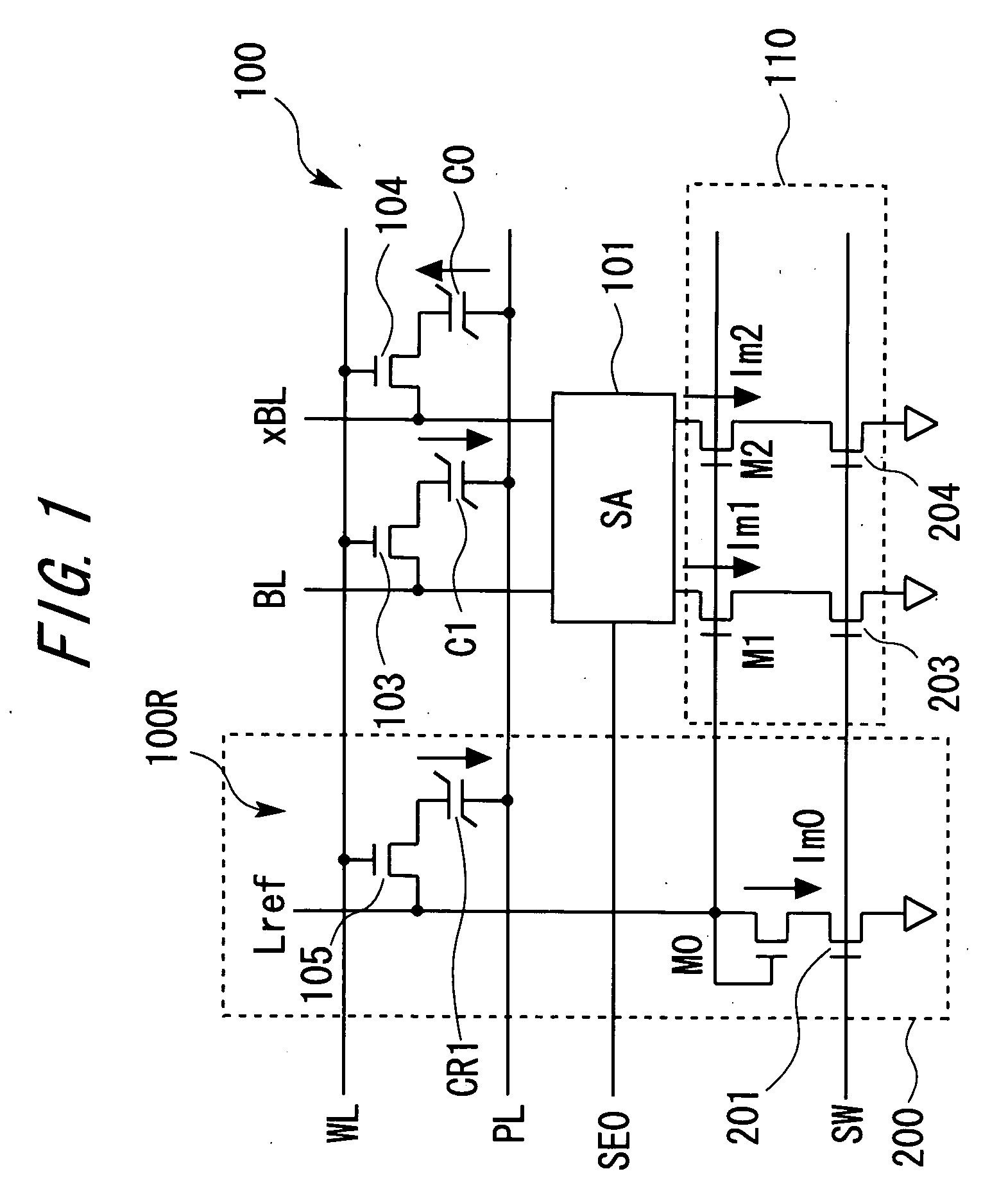
[0029]FIG. 11 is a circuit diagram showing an example of a configuration of the ferroelectric memory. This circuit includes ferroelectric capacitors C1 and C0 that store complementary data on each other, a bit line BL and a complementary bit line xBL that serve to input and output the data of the respective ferroelectric capacitors C1 and C0, an n-channel MOS (Metal-Oxide Semiconductor) field-effect transistor (FET) 103 that selectively connects the ferroelectric capacitor C1 and the bit line BL, an n-channel MOSFET 104 that selective connects the ferroelectric capacitor C0 and the complementary bit line xBL, a word line WL for controlling gate voltages of the n-channel MOSFETs 103 and 104, a plate line connected to a terminal on the opposite side to the n-channel MOSFET 103 (and 104) of the ferroelectric capacitor C1 (and C0), and a s...
second embodiment
[0104] A second embodiment of the invention will be described with reference to the drawings in FIGS. 8 through 10. In the first embodiment, the timing for activating the sense amplifier 101 detecting the potential difference ΔVBL between the bit line BL and the complementary bit line xBL of the memory cell, is determined in a way that detects the change in potential of the complementary reference bit line Tref when reading from the reference ferroelectric capacitor CR0.
[0105] In the case of such a configuration, an advantage is that the sense amplifier 101 can be activated at the timing when the potential difference ΔVBL between the bit line BL and the complementary bit line xBL keeps a value larger than the threshold voltage Vth in the case of the basic circuit (FIG. 1) from the change in potential of the complementary reference bit line Tref. In such a configuration, however, the characteristic of the reference ferroelectric capacitor CR0 or CR1 deteriorates, the hysteresis is w...
modified example
[0118] In the embodiments, the explanations have been made such that the n-type MOSFET is assumed to be each of the switching elements 103, 104, 105, 106, 201, 203, 204 and 211, and the switching element is switched ON when the gate voltage becomes the high level. The embodiment of the invention is not limited to this configuration. Namely, a p-type MOSFET that is switched ON at the low level may also be used as each of the switching elements.
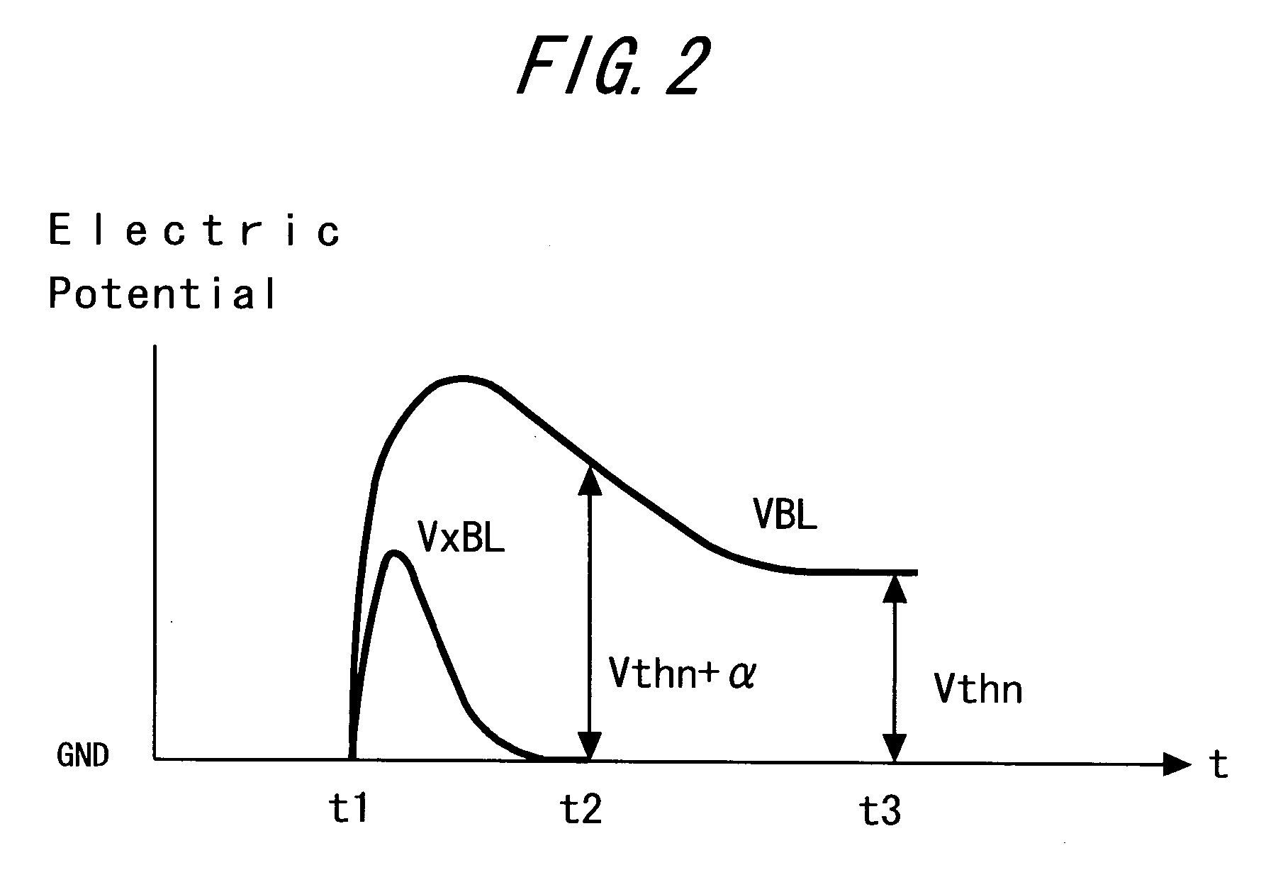
[0119] Further, if the timing for starting (activating) the sense (amplifier) exists, as obvious from FIG. 2, before stabilizing the potentials of the two bit lines to which the complementary data are outputted, the potential difference between these pieces of complementary data becomes large, thereby enabling the stable readout of the data. More desirably, the data can be read out more stably by detecting the potential difference between those pieces of complementary data in the vicinity of the timing when one of the two potentials of the com...
PUM
 Abstract
Description
Claims
Application Information


