Method for programming a memory device
- Summary
- Abstract
- Description
- Claims
- Application Information
AI Technical Summary
Benefits of technology
Problems solved by technology
Method used
Image

Examples
Embodiment Construction
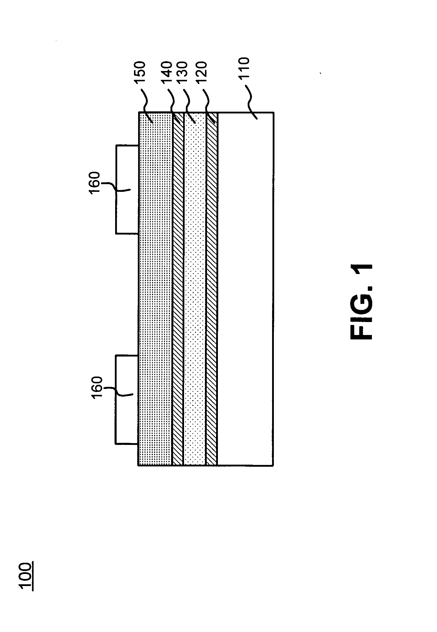
[0024]FIG. 1 illustrates the cross-section of a semiconductor device 100 formed in accordance with an embodiment of the invention. Referring to FIG. 1, semiconductor device 100 may include layers 110, 120, 130, 140 and 150. In an exemplary embodiment, layer 110 may be a substrate of semiconductor device 100 and may include silicon, germanium, silicon-germanium or other semiconducting materials. In alternative implementations, layer 110 may be a conductive layer or a dielectric layer formed a number of layers above the surface of a substrate in semiconductor device 100.
[0025] Layer 120 may be a dielectric layer formed on layer 110 in a conventional manner. In an exemplary implementation, dielectric layer 120 may include an oxide, such as a silicon oxide (e.g., SiO2), and may have a thickness ranging from about 30 Å to about 80 Å. Dielectric layer 120 may function as a tunnel oxide layer for a subsequently formed memory cell of semiconductor device 100.
[0026] Layer 130 may be formed...
PUM
 Abstract
Description
Claims
Application Information
 - Generate Ideas
- Intellectual Property
- Life Sciences
- Materials
- Tech Scout
- Unparalleled Data Quality
- Higher Quality Content
- 60% Fewer Hallucinations
Browse by: Latest US Patents, China's latest patents, Technical Efficacy Thesaurus, Application Domain, Technology Topic, Popular Technical Reports.
© 2025 PatSnap. All rights reserved.Legal|Privacy policy|Modern Slavery Act Transparency Statement|Sitemap|About US| Contact US: help@patsnap.com