
Device and manufacturing method thereof
- Summary
- Abstract
- Description
- Claims
- Application Information
AI Technical Summary
Benefits of technology
Problems solved by technology
Method used
Image

Examples
first embodiment
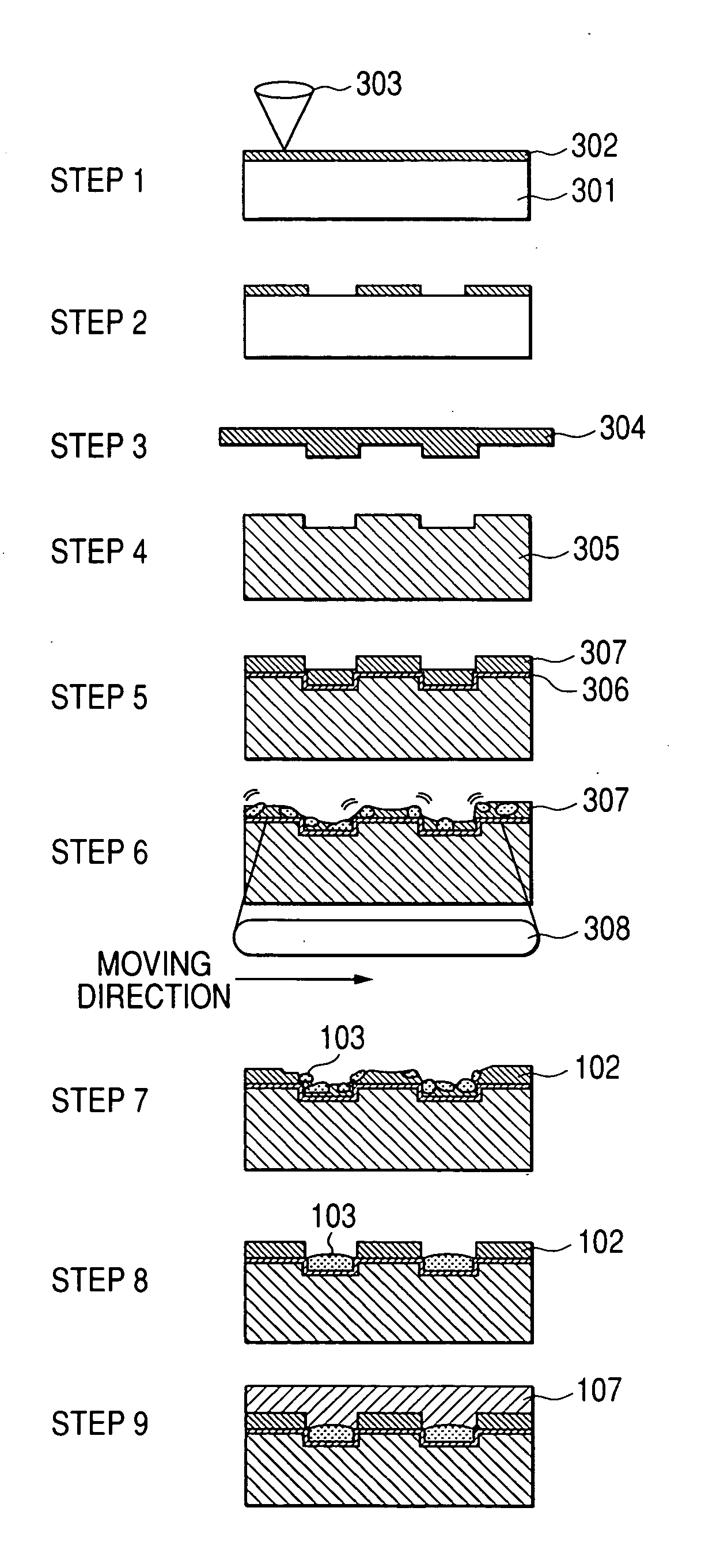
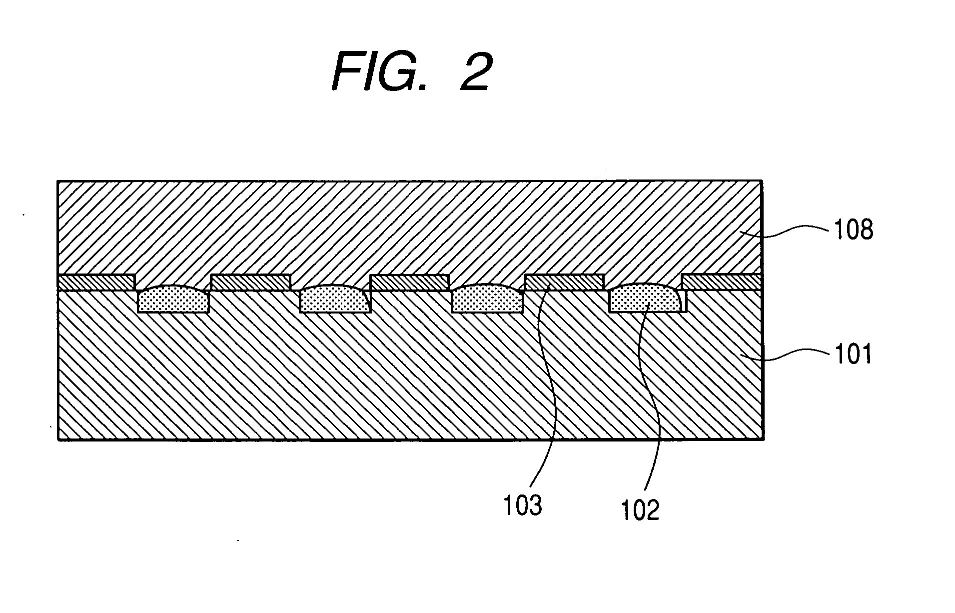
[0075] The first embodiment describes a manufacturing method of a ROM substrate using light. FIG. 2 is a cross-sectional structural drawing illustrating an example of a disk-shaped device in the present invention. This device has a structure, in which space parts mainly composed of the functional material C102 and mark parts mainly composed of the functional material B103 are segregated in the concave parts and the convex parts, respectively, on a substrate 101 having an uneven pattern on the surface, and the surface is covered with a protection substrate 108. FIG. 3 is an example of a method for forming the optical disk.
[0076] A pit pattern or line pattern shaped unevenly was formed by irradiating a focused laser beam 303 used for cutting onto the resist 302 coated on the glass substrate 301. Then, a Ni plate was formed by performing a plating technique on the surface, resulting in a Ni stamper 304 being fabricated. After that, a plastic substrate 305 having unevenness on the surf...
second embodiment
[0082]FIG. 5 is an example illustrating another method for manufacturing a substrate having an uneven shape. SOG (spin on glass) 402 is uniformly coated on a glass substrate 401, placed between a Ni stamper 304 and a glass plate and pressed, and peeled off at the interface with the Ni stamper by irradiating UV light 403, resulting in the pattern of the Ni stamper being transferred. The glass plate has excellent smoothness compared with a plastic substrate. Moreover, since SOG is mainly composed of SiO2, it has excellent thermal resistance and heating becomes possible by using a baking furnace instead of the aforementioned sheet beam. Furthermore, heating by using a baking furnace brings excellent productive efficiency since a plurality of pieces can be treated simultaneously. A 13 nm thick functional layer 307 composed of Au—Ge—Sb—Te was deposited by using a sputtering technique on a glass plate with SOG which has been transferred from the Ni stamper. Then, heat treatment is perform...
fourth embodiment
[0085] Another method for manufacturing a substrate having an uneven shape will be described. Even if it was a small trigger, it was effective for promoting the composition change in the functional layer. FIG. 7 is one example of a manufacturing method. First, an unevenly formed Ni stamper 304 was fabricated. The light for irradiating the resist is assumed to be an electron beam and a pit pattern with a diameter of 50 nm or a line pattern with a width of 50 nm was formed unevenly. As an example, a PMMA resin 701 was spin-coated on the glass substrate 301 and, after heating the whole substrate at 110° C., the Ni stamper was pressed onto the resin thin film in a vacuum atmosphere. The holding pressure was controlled to be 2 MPa. Then, while keeping the resin soft, the Ni stamper was peeled off from the substrate uniformly to elongate the resin and stretch in both the parallel and the vertical direction. As a result, the PMMA resin in the concave parts of the Ni stamper was elongated i...
PUM
 Abstract
Description
Claims
Application Information