MEMS switch and method for manufacturing the same

a micro-electromechanical system and switch technology, applied in the manufacture of relays, generators/motors, cable/conductor components, etc., can solve the problems of high driving voltage, poor uniformity of the structure manufactured in the wafer, and disadvantages of the mems switch performing its switching operation by electrostatic attraction, etc., to achieve stable contact force, enhance production yield, and manufacture in a high yield

Inactive Publication Date: 2007-01-18
SAMSUNG DISPLAY CO LTD
View PDF3 Cites 8 Cited by
  • Summary
  • Abstract
  • Description
  • Claims
  • Application Information

AI Technical Summary

Benefits of technology

[0014] An exemplary embodiment of the present invention provides a MEMS switch driven at a low voltage, having a stable contact force, and being capable of manufacture in a high yield, and a method for manufacturing the MEMS switch where the method is capable of enhancing a production yield by including a smaller number of process steps than conventional methods.

Problems solved by technology

However, MEMS switches performing their switching operations by electrostatic attraction have disadvantages as discussed below.
First, such conventional MEMS switches operate at a high driving voltage.
Second, in manufacturing the MEMS switches on a wafer, structures constituting the MEMS switches are not the same over the entire area of the wafer, that is, the uniformity of the structures manufactured in the wafer is not good.
Third, since the manufacturing method of the MEMS switches includes lots of process steps, the MEMS switches are manufactured in low yield.
Fourth, since a contact force of the contact member to the signal line is not stable, an insertion loss also increases as the number of switching operations increases.

Method used


Image

  • MEMS switch and method for manufacturing the same
  • MEMS switch and method for manufacturing the same
  • MEMS switch and method for manufacturing the same

Examples


Embodiment Construction

[0044] The present invention will now be described more fully hereinafter with reference to the accompanying drawings, in which exemplary embodiments of the invention are shown.

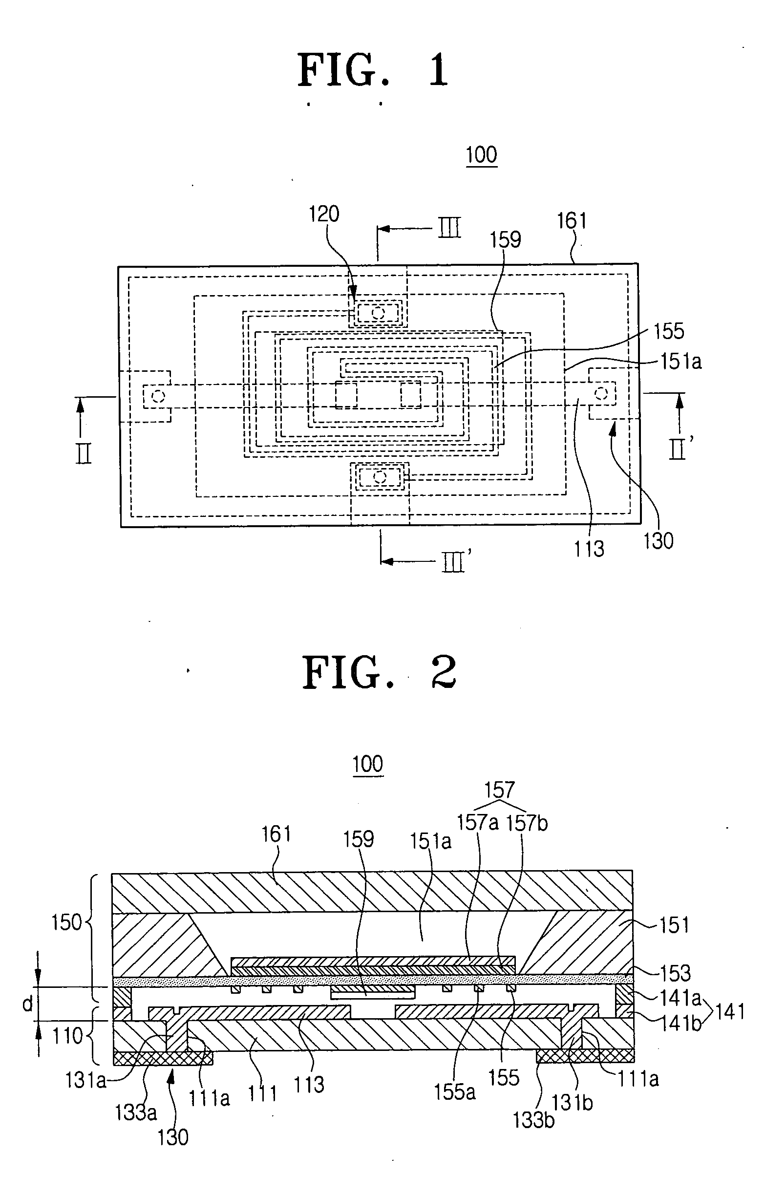
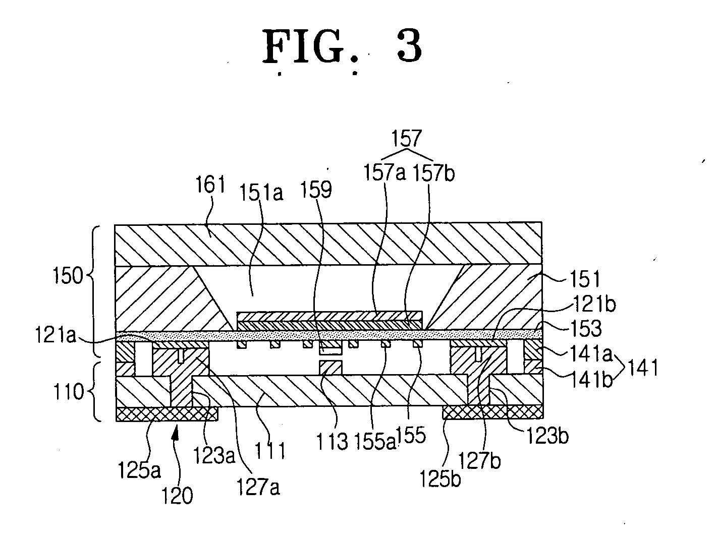
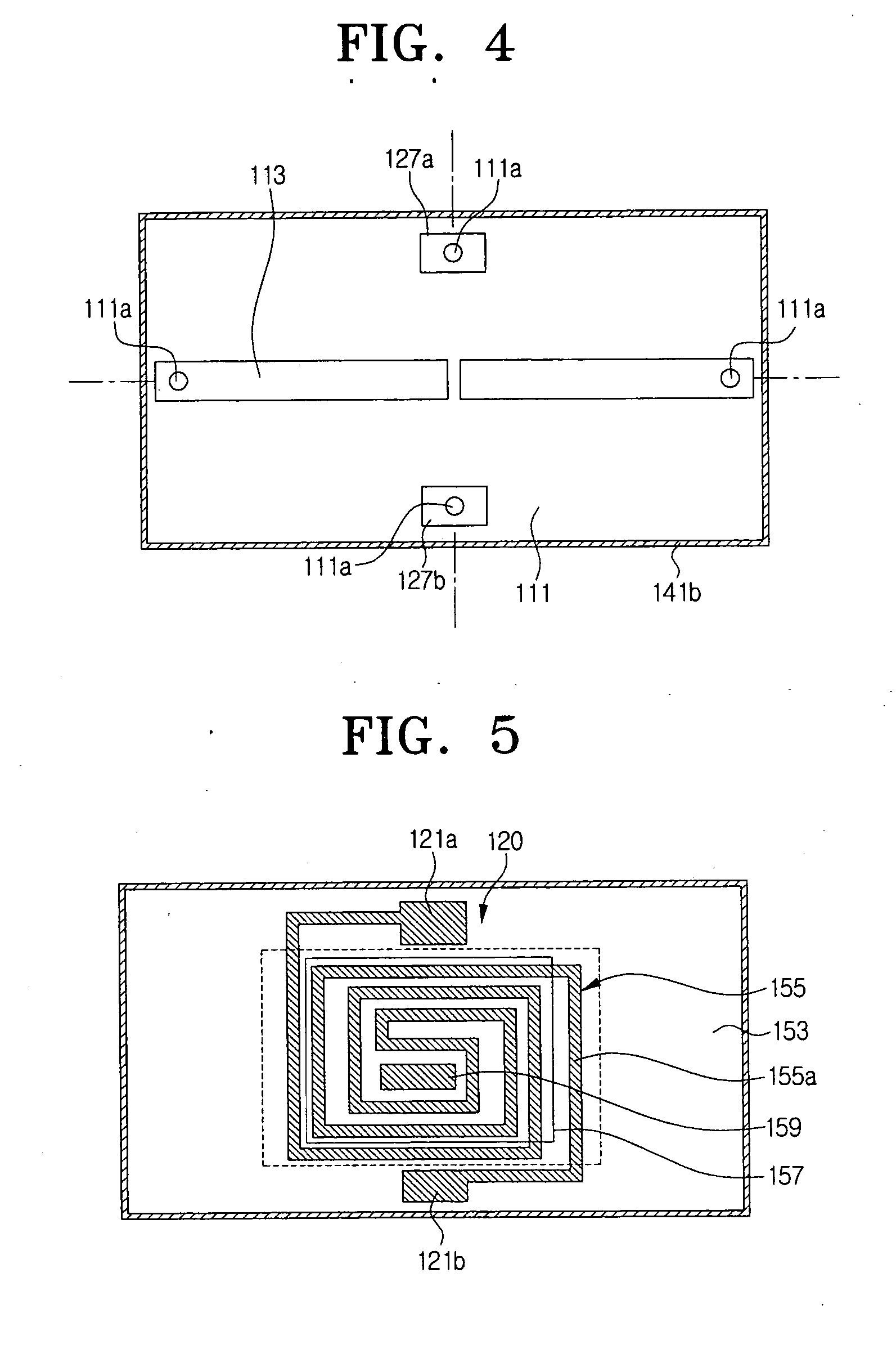
[0045]FIG. 1 illustrates a layout view of a MEMS switch according to one exemplary embodiment of the present invention, FIG. 2 illustrates a sectional view of the MEMS switch, where the view is taken along a line II-II′ shown in FIG. 1, and FIG. 3 illustrates a sectional view of the MEMS switch where the view is taken along a line III-III′ shown in FIG. 1.

[0046] Referring to FIGS. 1 to 3, the MEMS switch 100 includes a signal part 110 and a driving part 150.

[0047] The signal part 110 includes a lower substrate 111, a signal line 113 formed on an upper surface of the lower substrate 111, a signal line connection unit 130 for connecting external circuits, and a power supply unit 120 for supplying a voltage to a heating layer 155 in the driving part 150 to be described later. The lower substrate 111 may be ma...


PUM

PropertyMeasurementUnit
distanceaaaaaaaaaa
electrical resistanceaaaaaaaaaa
voltageaaaaaaaaaa

Abstract

A MEMS switch includes a lower substrate having a signal line on an upper surface of the lower substrate; an upper substrate, having a cavity therein, disposed apart from the upper surface of the lower substrate by a distance, and having a membrane layer on a lower surface of the upper substrate; a bimetal layer formed in the cavity of the upper substrate on the membrane layer; a heating layer formed on a lower surface of the membrane layer; and a contact member formed on a lower surface of the heating layer. The contact member can come into contact with or separate from the signal line. A method for manufacturing the MEMS switch includes preparing the upper and lower substrates and combining them so that a surface having the signal line faces a surface having the contact member and the upper and lower substrates are disposed apart by a distance.

Description

CROSS-REFERENCE TO RELATED APPLICATION [0001] This application claims priority from Korean Patent Application No. 10-2005-0064798 filed on Jul. 18, 2005, the entire contents of which are incorporated herein by reference. BACKGROUND OF THE INVENTION [0002] 1. Field of the Invention [0003] Apparatuses and methods consistent with the present invention relate to a Micro-Electro-Mechanical Systems (MEMS) switch and a method for manufacturing the same. [0004] 2. Description of the Related Art [0005] Electronic systems for use in a high frequency bandwidth are getting slimmer, smaller, lighter, and better in performance. Ultra-small microswitches using a new technology such as micromachining are being developed to substitute for semiconductor devices such as Field Effect Transistors (FET) and pin diodes, which have been used for controlling such electronic systems. [0006] Among radio frequency (RF) devices using MEMS technologies, most devices manufactured are switches. RF switches are fre...

Claims


Application Information

Patent Timeline
Patent Type & Authority Applications(United States)
IPC IPC(8): C23F1/00H01B13/00
CPCH01H61/02H01H61/063H01H2061/006H01L29/00
Inventor KIM, JONG-SEOKSONG, IN-SANGLEE, SANG-HUNKWON, SANG-WOOKKIM, DUCK-HWANPARK, YUN-KWONJEONG, HEE-MOONHONG, YOUNG-TACKKIM, CHE-HEUNGYUN, SEOK-CHULNAM, KUANG-WOO
Owner SAMSUNG DISPLAY CO LTD
Why Eureka
Try Eureka