Bipolar transistor and power amplifier

a power amplifier and bipolar transistor technology, applied in the field of bipolar transistors and power amplifiers, can solve the problems of deterioration of radio frequency characteristics, failure of hbt cell operation, and occupying the emitter finger of a semiconductor chip, so as to reduce the chip area, improve the gain characteristics of a radio frequency band, and uniform heat generation

Active Publication Date: 2007-01-18
PANASONIC SEMICON SOLUTIONS CO LTD
View PDF8 Cites 19 Cited by
  • Summary
  • Abstract
  • Description
  • Claims
  • Application Information

AI Technical Summary

Benefits of technology

[0016] Therefore, an object of the present invention is to provide a bipolar transistor which has uniform heat generation in an HBT cell and improves gain characteristics in a radio frequency band, and a power amplifier which employs a multi-cell structure to reduce a chip area.

Problems solved by technology

However, the emitter finger needlessly occupies a semiconductor chip area.
However, the HBT cells do not uniformly generate heat, so that a failure occurs in the operation of the HBT cell due to non-uniformity of heat generation between each HBT cell.
More specifically, the HBT cell having a temperature higher than the surrounding having a high increase in temperature further generates heat due to positive feedback (thermal runaway), finally leading to breakdown.
Also, when heat generation is not uniform between each HBT cell, none of the HBT emitters effectively functions, resulting in a deterioration in radio frequency characteristics.
As described above, the conventional power-amplification HBT employing a base ballast resistance takes measures against the non-uniformity of heat generation between each HBT cell, however, the non-uniformity of heat generation in each HBT cell is not taken into consideration.
In this case, however, the area of the HBT cell is increased, resulting in newly arising problems: an increase in chip area; a deterioration in radio frequency characteristics; and the like.
Therefore, it is not practical.
In the case of the HBT cell of FIG. 11A, since the five base fingers are provided on both the sides of the four emitter fingers, non-uniformity is likely to occur between each finger in terms of a contact resistance of the base electrode and the base layer of each base finger.
Therefore, non-uniformity occurs in the injection amount of a base current, resulting in non-uniformity between each emitter finger.
This problem similarly exists in the HBT cell having one emitter finger and two base fingers of FIG. 10A.
Specifically, non-uniformity is likely to occur between the two base fingers in terms of a contact resistance of the base electrode and the base layer of the two base fingers.
Due to non-uniformity of the base resistances of both the sides, non-uniformity in the operation of the HBT cell increases.
Further, in the HBT cell, a base-collector parasitic capacitance is high, and power feedback due to the parasitic capacitance causes a gain deterioration in radio frequency band applications.
Thus, in the conventional HBT cell structure, there is a limitation on the reduction of the base mesa width W1 due to the influence of the base finger, resulting in a deterioration in gain characteristics in a radio frequency band.
Therefore, when the power-amplification HBT is actually integrated on a semiconductor, a large area needs to be secured for an external base resistance, resulting in a large chip area, i.e., an increase in cost.

Method used


Image

  • Bipolar transistor and power amplifier
  • Bipolar transistor and power amplifier
  • Bipolar transistor and power amplifier

Examples


Embodiment Construction

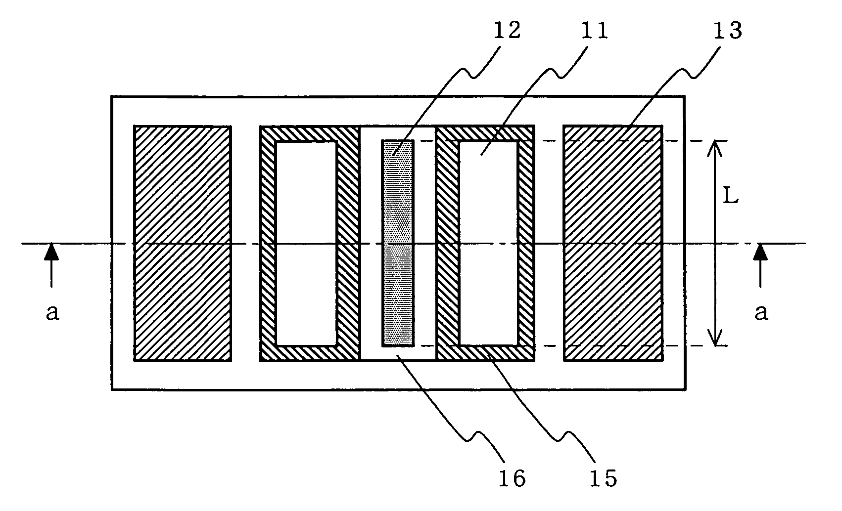
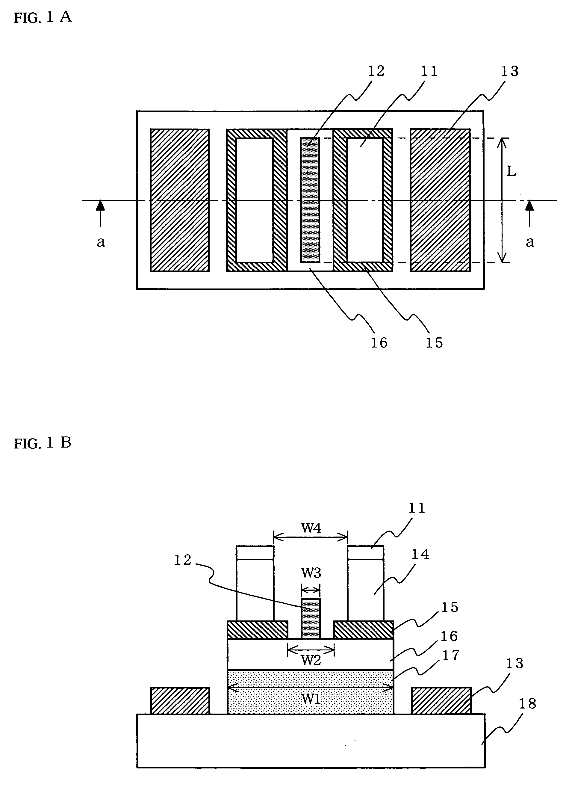
[0042] (Structure of Bipolar Transistor)

[0043] Initially, a structure of a bipolar transistor according to an embodiment of the present invention will be described.

[0044]FIG. 1A is a plan view illustrating the structure of the bipolar transistor according to the embodiment of the present invention. FIG. 1B is a cross-sectional view illustrating the bipolar transistor, taken along line a—a in FIG. 1A. In the structure of the bipolar transistor of this embodiment, a base mesa finger (an emitter ledge layer 15, a base layer 16, and a collector layer 17) is interposed between two collector fingers (collector electrodes 13), and one base finger (a base electrode 12) and two emitter fingers (an emitter layer 14 and an emitter electrode 11) on both sides of the base finger, are formed on the base mesa finger. The two emitter fingers are formed at locations symmetric with respect to the base finger as a reference. This bipolar transistor is typically a heterojunction bipolar transistor (H...


PUM


Abstract

A base mesa finger (an emitter ledge layer 15, a base layer 16, and a collector layer 17) is interposed between two collector fingers (collector electrodes 13), and on the base mesa finger, a base finger (a base electrode 12) and two emitter fingers (an emitter layer 14 and an emitter electrode 11) on both sides of the base finger, are formed. The two emitter fingers are formed symmetric with respect to the base finger as a reference.

Description

BACKGROUND OF THE INVENTION [0001] 1. Field of the Invention [0002] The present invention relates to a bipolar transistor and a power amplifier. More particularly, the present invention relates to a bipolar transistor which is formed as an active element on a semiconductor integrated circuit for power amplification which is used in a signal transmitting section of a mobile radio terminal (a mobile telephone, etc.) which uses a radio frequency band, and a power amplifier employing the bipolar transistor. [0003] 2. Description of the Background Art [0004] In recent years, a semiconductor integrated circuit for power amplification which employs, as an active element, a bipolar transistor made of a compound semiconductor which enables a radio frequency operation and a positive power supply operation, is widely used in a signal transmitting section of a mobile radio terminal, such as a mobile telephone or the like. Particularly, a heterojunction bipolar transistor (hereinafter abbreviate...

Claims


Application Information

Patent Timeline
Patent Type & Authority Applications(United States)
IPC IPC(8): H01L31/00H01L21/336
CPCH01L29/0692H01L29/41708H01L29/7371H01L29/66318H01L29/42304
Inventor KAWASHIMA, KATSUHIKOMAEDA, MASAHIROMURAYAMA, KEIICHIMIYAMOTO, HIROTAKA
Owner PANASONIC SEMICON SOLUTIONS CO LTD
Why Eureka
Try Eureka