Memory device
a memory device and memory technology, applied in the field of memory devices, can solve the problems of increased consumption current, difficulty in and difficulty in memory device high-speed driving, so as to achieve easy patterning in memory element manufacturing and high-speed driving of memory elements
- Summary
- Abstract
- Description
- Claims
- Application Information
AI Technical Summary
Benefits of technology
Problems solved by technology
Method used
Image
Examples
first embodiment
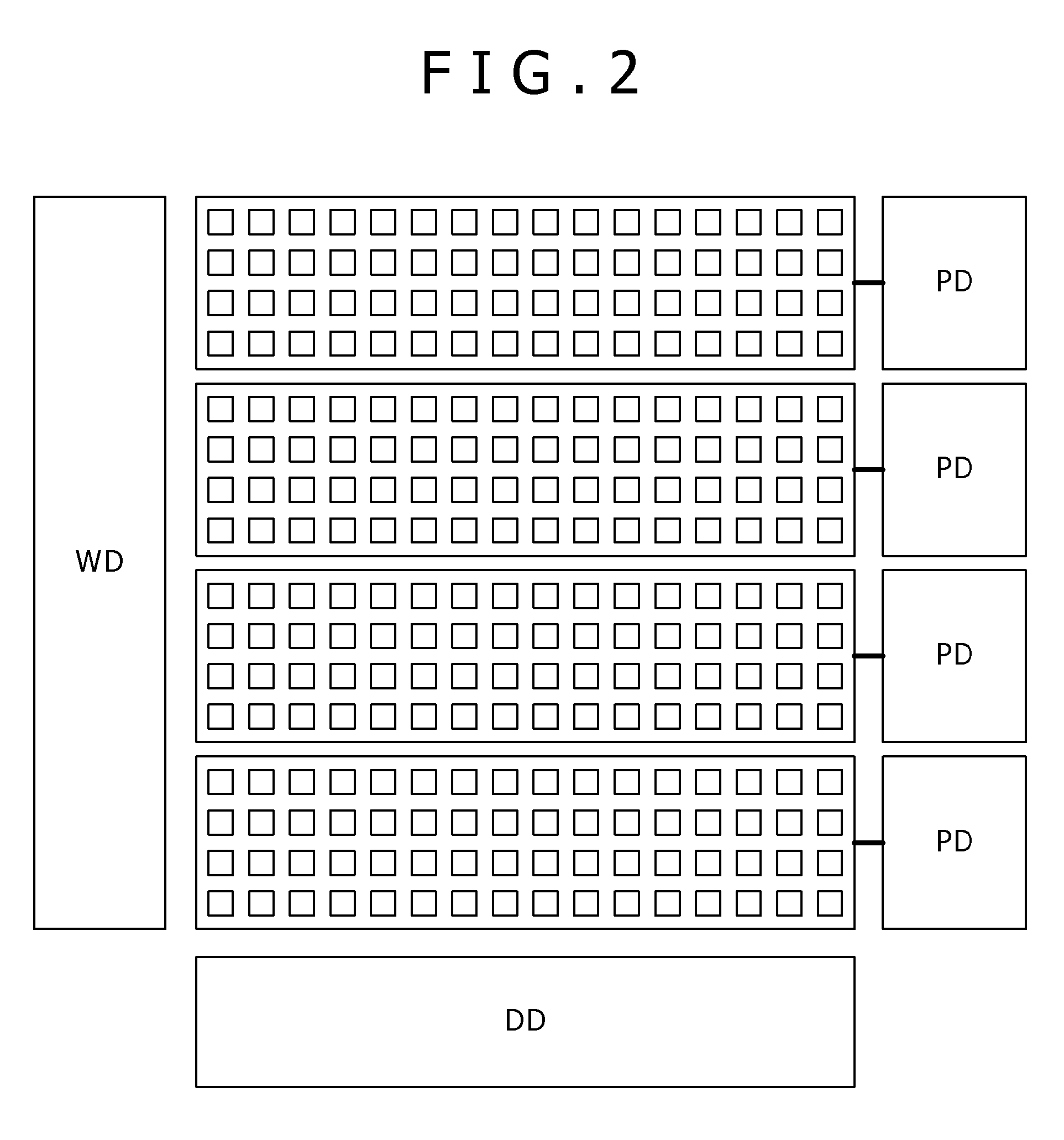
[0085]FIG. 2 is a schematic diagram for explaining a memory device in which each unit memory block includes memory cells of horizontal 16 bits by vertical 4 bits.
[0086] In the memory device shown in the drawing, a memory array of 256 bits includes four unit memory blocks each having memory cells of horizontal 16 bits by vertical 4 bits, and the four memory blocks are arranged along the vertical direction. The memory elements of the memory cells in each unit memory block (horizontal 16 bits by vertical 4 bits) are formed of a single high resistance film, a single ion source layer and a single upper electrode. Specifically, in the first embodiment, a single plate is quadrisected along the vertical direction so that four separated plates are formed.
[0087] The word lines are connected to a word driver WD, and the bit lines are connected to a data driver DD. Each of the upper electrodes of the respective separated plates is connected to a corresponding plate driver PD. Specifically, th...
second embodiment
[0090]FIG. 3 is a schematic diagram for explaining a memory device in which each unit memory block includes memory cells of horizontal 4 bits by vertical 16 bits.
[0091] In the memory device shown in the drawing, a memory array of 256 bits includes four unit memory blocks each having memory cells of horizontal 4 bits by vertical 16 bits, and the four memory blocks are arranged along the horizontal direction. The memory elements of the memory cells in each unit memory block (horizontal 4 bits by vertical 16 bits) are formed of a single high resistance film, a single ion source layer and a single upper electrode. Specifically, in the second embodiment, a single plate is quadrisected along the horizontal direction so that four separated plates are formed.
[0092] The word lines are connected to a word driver WD, and the bit lines are connected to a data driver DD. Each of the upper electrodes of the respective separated plates is connected to a corresponding plate driver PD. Specificall...
third embodiment
[0097]FIG. 4 is a schematic diagram for explaining a memory device in which each unit memory block includes memory cells of horizontal 4 bits by vertical 4 bits.
[0098] In the memory device shown in the drawing, a memory array of 256 bits includes 16 (horizontal 4 by vertical 4) unit memory blocks each having memory cells of horizontal 4 bits by vertical 4 bits. The memory elements of the memory cells in each unit memory block (horizontal 4 bits by vertical 4 bits) are formed of a single high resistance film, a single ion source layer and a single upper electrode. Specifically, in the third embodiment, a single plate is quadrisected along the vertical and horizontal directions, respectively, so that 16 separated plates are formed.
[0099] The word lines are connected to a word driver WD, and the bit lines are connected to a data driver DD. Each of the upper electrodes of the respective separated plates is connected to a corresponding plate driver PD. Specifically, the upper electrode...
PUM
 Abstract
Description
Claims
Application Information


