Method for manufacturing semiconductor apparatus and the semiconductor apparatus

a manufacturing method and semiconductor technology, applied in the direction of semiconductor devices, electrical devices, basic electric elements, etc., can solve the problems of deteriorating the performance and reliability of devices, deteriorating the pressure resistance, and so on transistors, so as to suppress the generation of defective crystallization, and reduce the burden on the apparatus to the environment

Inactive Publication Date: 2007-01-25
SEIKO EPSON CORP
View PDF1 Cites 11 Cited by
  • Summary
  • Abstract
  • Description
  • Claims
  • Application Information

AI Technical Summary

Benefits of technology

[0014] An advantage of the invention is to provide a method for manufacturing a semiconductor apparatus having a DSOI transistor by which a special production apparatus and burden by the apparatus to environment are reduced to suppress the generation of defective crystallization during the manufacture, and the semiconductor apparatus.
[0015] According to a first aspect of the Invention, a method for manufacturing a semiconductor apparatus includes: forming a first semiconductor layer on a semiconductor substrate of a transistor formation region; etching and removing a part of the first semiconductor layer sandwiched by a source formation region and a drain formation region to form a groove section in which a surface of the semiconductor substrate is exposed in the first semiconductor layer; forming a second semiconductor layer having an etching selectivity smaller than that of the first semiconductor layer on the semiconductor substrate of the transistor formation region so that the groove section is filled and the surface of the first semiconductor layer is covered; etching and removing the first semiconductor layer under the second semiconductor layer from the outside of the transistor formation region to form a cavity section under the second semiconductor layer; and forming a buried oxide film in the cavity section.
[0016] The term “semiconductor substrate” here represents, for example, a bulk silicon (Si) substrate and the term “the first semiconductor layer” represents, for example, a silicon germanium (SiGe) layer. The term “the second semiconductor layer” represents, for example, a Si layer. The first semiconductor layer and the second semiconductor layer as described above are formed by the epitaxial growth method for example.
[0017] The method for manufacturing a semiconductor apparatus of the first aspect of the invention can eliminate the need for a special production apparatus as used in the SIMOX method (e.g., HOT-impra apparatus, high temperature anneal furnace). Thus, a DSOI transistor that suppresses the generation of defective crystallization during the manufacture can be provided with a low cost and without causing a burden to an environment by the consumption of a large amount of electric power.
[0018] According to a second aspect of the invention, a method for manufacturing a semiconductor apparatus includes: forming a first semiconductor layer on a semiconductor substrate; etching and removing a part of the first semiconductor layer sandwiched by a source formation region and a drain formation region to form a groove section in which a surface of the semiconductor substrate is exposed in the first semiconductor layer; forming a second semiconductor layer having an etching selectivity smaller than that of the first semiconductor layer on the semiconductor substrate so that the groove section is filled and the surface of the first semiconductor layer is covered; sequentially etching and removing the second semiconductor layer exterior to a transistor formation region and the first semiconductor layer exterior to the second semiconductor layer to expose an end section of the first semiconductor layer along the periphery of the transistor formation region; etching and removing the first semiconductor layer from the exposed end section to form a cavity section under the second semiconductor layer of the transistor formation region; and forming a buried oxide film in the cavity section.
[0019] The structure as described above can eliminate the need for a special production apparatus as used in the SIMOX method (e.g., HOT-impra apparatus, high temperature anneal furnace). Thus, a DSOI transistor that suppresses the generation of defective crystallization during the manufacture can be provided with a low cost and without causing a burden to an environment by the consumption of a large amount of electric power.

Problems solved by technology

This phenomenon is called as a self-heat effect that is one of causing factors of deteriorating the performance and reliability of the device.
The SOI transistor has another problem of a substrate floating effect.
This effect causes influences according to one of which an end of a drain of an Nch transistor for example has a hole due to the impact ion and this hole is accumulated in the body, which deteriorates the pressure resistance.
In other words, the above method has required special apparatuses for performing the SIMOX method and electric power for operating them, which causes an increased cost and a larger burden to environment (problem 1).
Furthermore, the above method for manufacturing a DSOI transistor has caused a risk in which the oxygen ion implantation with a high concentration may cause defective crystallization in a Si substrate and this defect may cause an adverse effect on the device characteristic (problem 2).

Method used


Image

  • Method for manufacturing semiconductor apparatus and the semiconductor apparatus
  • Method for manufacturing semiconductor apparatus and the semiconductor apparatus
  • Method for manufacturing semiconductor apparatus and the semiconductor apparatus

Examples


Embodiment Construction

[0037] Hereinafter, embodiments of the invention will be described with reference to the drawings.

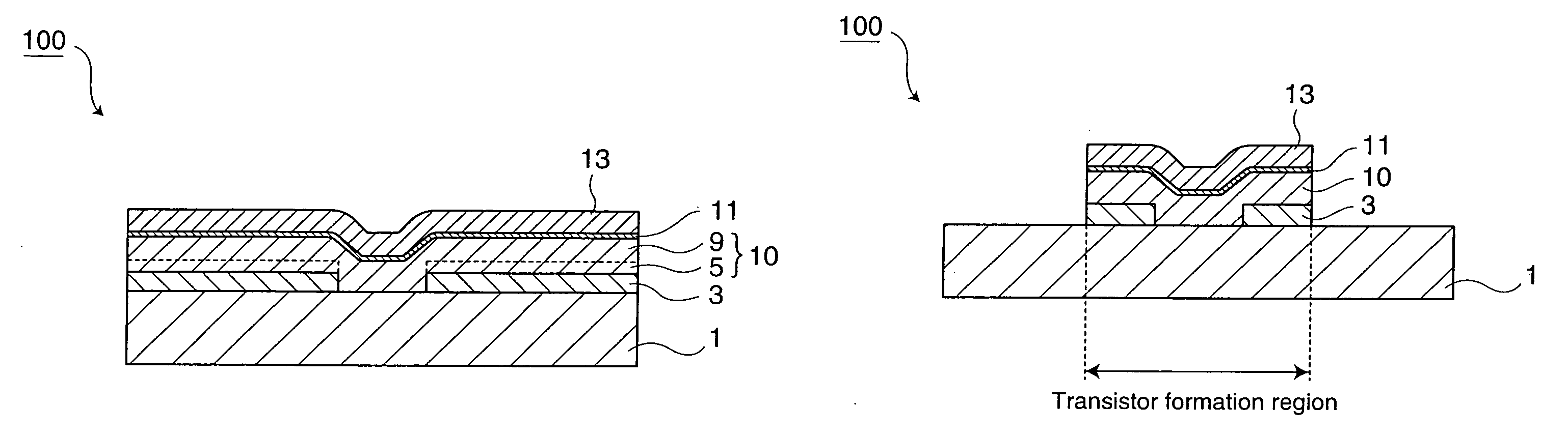
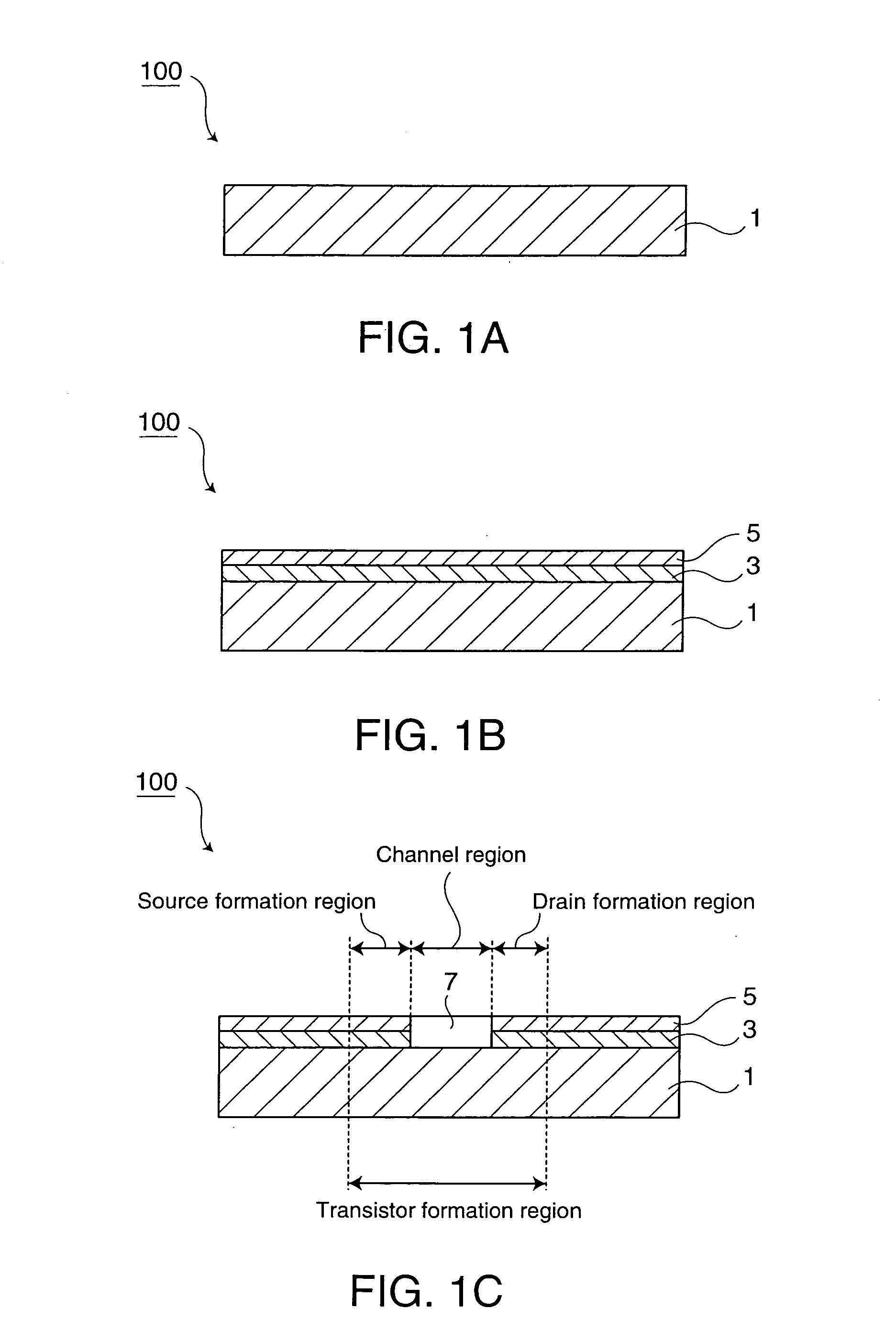
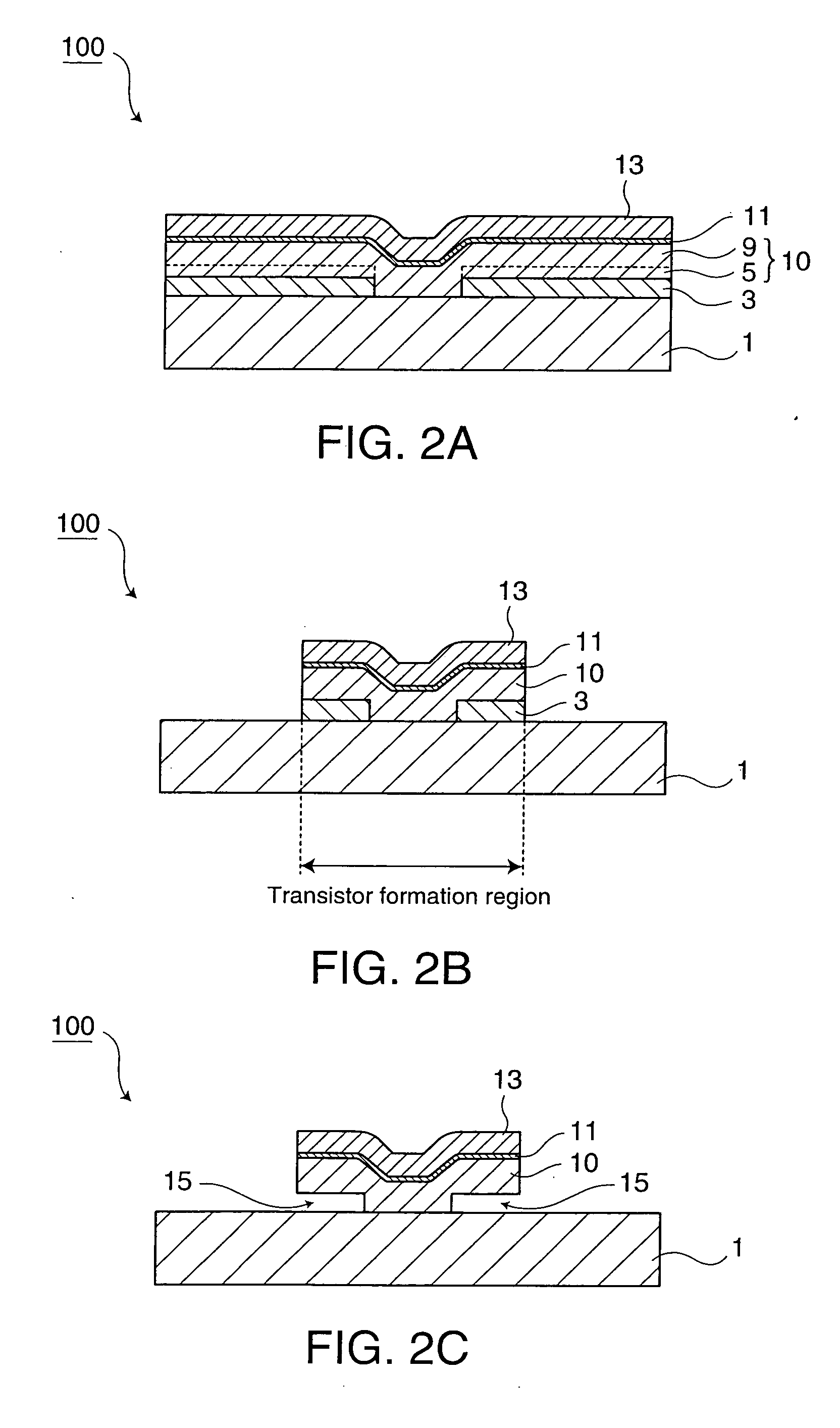
[0038]FIG. 1A to FIG. 3C are a cross-sectional view illustrating a method for manufacturing a semiconductor apparatus according to embodiments of the invention.

[0039] As shown in FIG. 1A, a Si substrate 1 as a bulk silicon wafer is prepared. Next, as shown in FIG. 1B, a SiGe layer 3 is formed on this Si substrate 1 and a first Si layer 5 is formed on the SiGe layer 3. The SiGe layer 3 and the Si layer 5 are formed by the epitaxial growth method (or selective epitaxial growth method), respectively.

[0040] When the Si substrate 1 is subjected to a dry etching processing prior to the formation of the SiGe layer 3, the dry etching processing may cause damage to the Si substrate 1. In order to remove this damage, the surface of the Si substrate 1 may be slightly oxidized prior to the formation of the SiGe layer 3 to subsequently remove the oxide film by a wet etching.

[0041] Next, as shown...


PUM


Abstract

A method for manufacturing a semiconductor apparatus, comprises: forming a first semiconductor layer on a semiconductor substrate of a transistor formation region; etching and removing a part of the first semiconductor layer sandwiched by a source formation region and a drain formation region to form a groove section in which a surface of the semiconductor substrate is exposed in the first semiconductor layer; forming a second semiconductor layer having an etching selectivity smaller than that of the first semiconductor layer on the semiconductor substrate of the transistor formation region so that the groove section is filled and the surface of the first semiconductor layer is covered; etching and removing the first semiconductor layer under the second semiconductor layer from the outside of the transistor formation region to form a cavity section under the second semiconductor layer; and forming a buried oxide film in the cavity section.

Description

BACKGROUND OF THE INVENTION [0001] 1. Technical Field [0002] The present invention relates to a method for manufacturing a semiconductor apparatus and the semiconductor apparatus. In particular, the invention relates to a method for manufacturing a semiconductor apparatus and the semiconductor apparatus by which the generation of defective crystallization during the manufacture can be suppressed without requiring a special production apparatus. [0003] 2. Related Art [0004] A field effect type transistor formed on an silicon on insulator (SOI) substrate (hereinafter referred to as “SOI transistor”) has attracted attention for the usefulness because elements can be separated easily, it is latchup free, and it has a small sourcedrain junction capacity for example. A complete depletion type SOI transistor in particular, which consumes a low power and can be operated with a high speed and can be easily driven with a low voltage, has been actively researched in order to operate the SOI tr...

Claims


Application Information

Patent Timeline
Patent Type & Authority Applications(United States)
IPC IPC(8): H01L21/84H01L21/00
CPCH01L29/0653H01L21/18
Inventor HARA, TOSHIKI
Owner SEIKO EPSON CORP
Why Eureka
Try Eureka