Electronic device and method for manufacturing the electronic device

a technology of electronic devices and manufacturing methods, applied in the direction of semiconductor devices, semiconductor/solid-state device details, electrical apparatus, etc., can solve the problems of peeling of bonding pads, poor contact of films with substrate surface layers, etc., and achieve high reliability of electronic devices, superior peeling resistance, and high productivity

Inactive Publication Date: 2007-02-01
SEIKO EPSON CORP
View PDF10 Cites 7 Cited by
  • Summary
  • Abstract
  • Description
  • Claims
  • Application Information

AI Technical Summary

Benefits of technology

[0007] An advantage of the invention is to provide a method for manufacturing a highly reliable electronic device with a high productivity and an electronic device manufactured by this manufacture method.
[0008] According to an aspect of the invention, a method for manufacturing an electronic device in which a bonding pad composed of a foundation layer and a surface layer is formed on an Si layer or an Si-base insulation layer, includes: forming, on the Si layer or Si-base insulation layer and by a droplet discharging method, the foundation layer using liquid material including one or more material(s) selected from Ni, Cr, and Mn or a compound thereof, and forming, on the foundation layer and by the droplet discharging method, the surface layer.
[0009] According to the method for manufacturing an electronic device, a foundation layer having a preferred contact to the Si layer or an Si-base insulation layer is formed to subsequently form a surface layer on the foundation layer. Thus, a bonding pad having a superior peeling resistance can be formed. Furthermore, liquid material including Ni, Cr, and Mn or an oxide thereof used for the formation of the foundation layer is well matched with the droplet discharging method, thus reducing burdening factors in steps related to the droplet discharging. In this manner, a highly reliable electronic device can be manufactured with a high productivity.
[0010] It is preferable that, according to the method for manufacturing an electronic device of the invention, the surface layer is formed by liquid material including one or more particle(s) or a compound material selected from Au, Ag, and Cu.
[0011] According to the method for manufacturing an electronic device of the invention, the liquid material including Au, Ag, or Cu particles constituting the surface layer is well matched with the droplet discharging method and thus reduces burdening factors in steps related to the droplet discharging.
[0012] According to another aspect of the invention, an electronic device in which a bonding pad composed of a foundation layer and a surface layer is formed on an Si layer or an Si-base insulation layer, wherein: the foundation layer is formed on the Si layer or Si-base insulation layer by the droplet discharging method using liquid material including one or more material(s) selected from Ni, Cr, and Mn or a compound thereof; and the surface layer is formed on the foundation layer by the droplet discharging method.

Problems solved by technology

However, a film formed by the droplet discharging method consists of collection of particles of functional material and thus is generally inconvenient in that this film has poor contact with a surface layer of a substrate when compared with a film formed by the gas phase method for example.
This has caused an inconvenience where, when a bonding pad is formed by Au having a preferred electric property and having a superior liquid material for example, the resultant bonding pad has an insufficient contact strength with a surface layer of a substrate, causing stress in wire bonding to peel the bonding pad from the surface layer of the substrate.

Method used


Image

  • Electronic device and method for manufacturing the electronic device
  • Electronic device and method for manufacturing the electronic device
  • Electronic device and method for manufacturing the electronic device

Examples


first embodiment

[0022] (Structure of Electronic Device)

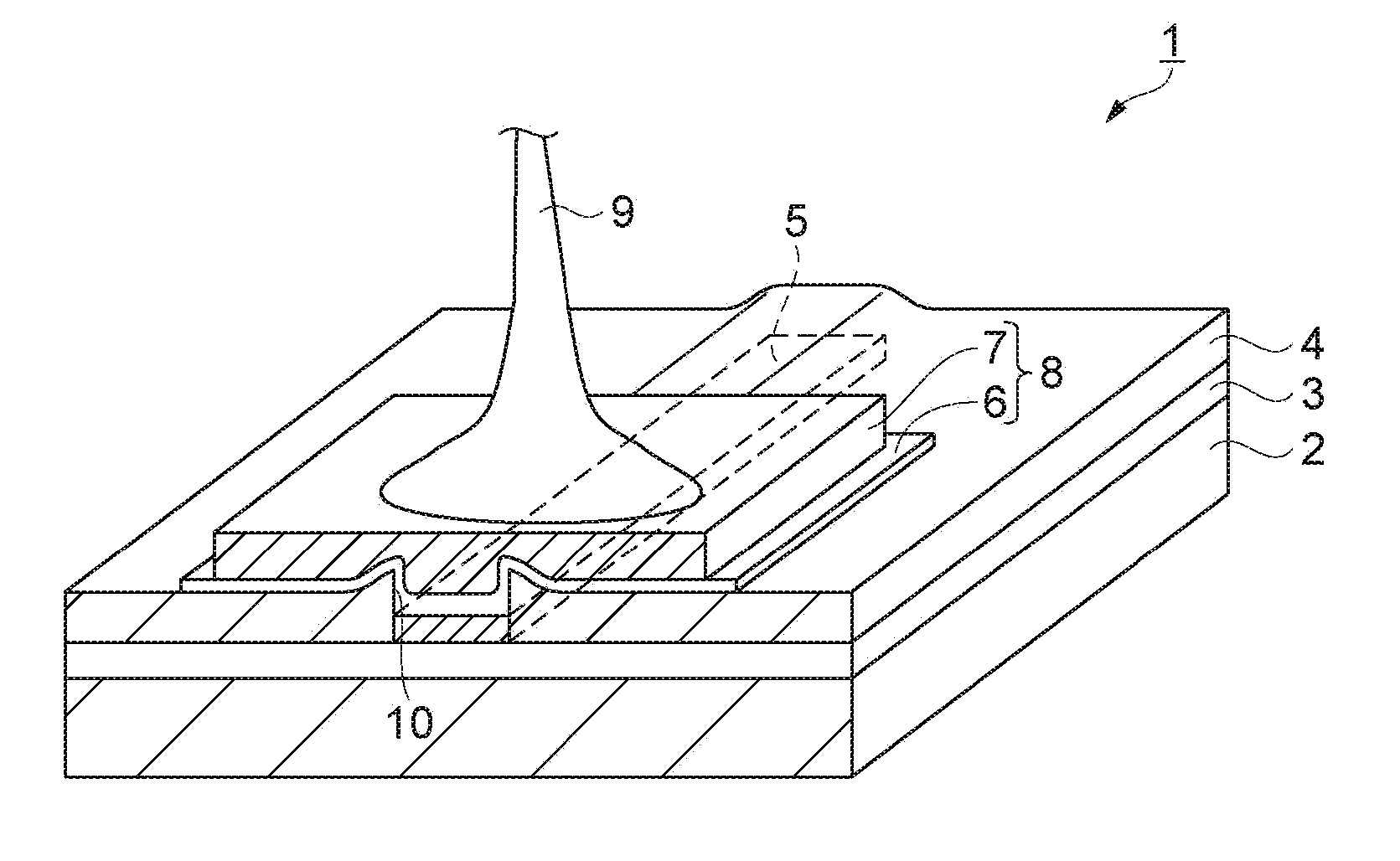
[0023] First, an electronic device according to First Embodiment will be described with reference to FIG. 1. FIG. 1 is a partially broken perspective view illustrating a main structure of the electronic device according to First Embodiment.

[0024] In FIG. 1, an integrated circuit 1 as an electronic device includes: a silicon substrate 2 including a semiconductor element (not shown); an insulation layer 3 that is formed on the silicon substrate 2 and that is made of BPSG (Boron-doped Phospho Silicate Glass) or the like; a conductive wiring 5 that is connected to the semiconductor element and that is made of Al or the like; and a covering layer 4 that covers the conductive wiring 5 and that is made of SiO2, SiN or the like. The covering layer 4 has thereon a bonding pad 8 connected to the covering layer 4 via the conductive wiring 5 and a contact hole 10. The bonding pad 8 is connected to a lead frame (not shown) via a bonding wire 9.

[0025] The...

second embodiment

[0050] The following section will describe Second Embodiment of the invention with reference to FIG. 5 mainly with regards to the difference between Second Embodiment and First Embodiment. FIG. 5 is a partially broken perspective view illustrating the main structure of an electronic device of Second Embodiment.

[0051] In FIG. 5, an integrated circuit 20 as an electronic device includes: a silicon substrate 21 including a semiconductor element (not shown); an insulation layer 22 as an Si-base insulation layer formed on the silicon substrate 21; a bank layer 23; and a conductive wiring 25 and a bonding pad 26 integrally formed by the droplet discharging method. The bank layer 23 is made of photosensitive resin for example and is patterned by the photolithography technique so that regions in which the conductive wiring 25 and the bonding pad 26 are formed can be divided.

[0052] The conductive wiring 25 and the bonding pad 26 have a layered structure composed of an Ni-made foundation la...


PUM

PropertyMeasurementUnit
thicknessaaaaaaaaaa
particle sizeaaaaaaaaaa
electric propertyaaaaaaaaaa

Abstract

A method for manufacturing an electronic device in which a bonding pad composed of a foundation layer and a surface layer is formed on an Si layer or an Si-base insulation layer, comprises: forming, on the Si layer or Si-base insulation layer and by a droplet discharging method, the foundation layer using liquid material including one or more material(s) selected from Ni, Cr, and Mn or a compound thereof; and forming, on the foundation layer and by the droplet discharging method, the surface layer.

Description

BACKGROUND [0001] 1. Technical Field [0002] The present invention relates to an electronic device such as a semiconductor integrated circuit or a semiconductor sensor and a manufacture method thereof. [0003] 2. Related Art [0004] Recently, a method for manufacturing an electronic device has been known in which a minute conducting wire pattern or a circuit element for example is formed by the so-called droplet discharging method (see JP-A-2003-317945 for example). This technique is a technique in which a droplet discharging head as used in an ink discharge printer is used to discharge liquid material including particles of functional material onto a substrate to subsequently solidify (or form a film of) the liquid material by drying or the like. When compared with the photolithography method as a general patterning technique, the droplet discharging method has a simple process and provides a superior efficiency of the use of functional material and thus has attracted attention as a t...

Claims


Application Information

Patent Timeline
Patent Type & Authority Applications(United States)
IPC IPC(8): H01L29/40H01L21/44
CPCH01L24/03H01L2924/01024H01L24/48H01L2224/02166H01L2224/04042H01L2224/05073H01L2224/05639H01L2224/05644H01L2224/05647H01L2224/48463H01L2224/85399H01L2924/01004H01L2924/01005H01L2924/01007H01L2924/01013H01L2924/01014H01L2924/01025H01L2924/01028H01L2924/01029H01L2924/01033H01L2924/01047H01L2924/01078H01L2924/01079H01L2924/01082H01L2924/14H01L24/05H01L2924/01006H01L2924/00014H01L2224/023H01L2224/45099H01L2224/05599H01L2924/0001
Inventor MORIYAMA, HIDEKAZU
Owner SEIKO EPSON CORP
Why Eureka
Try Eureka