

Integrated sensor and circuitry and process therefor
a sensor and circuitry technology, applied in the field of micromachined semiconductor sensors, can solve the problems of a large mechanical noise floor, a relatively large parasitic load, and a tens to hundreds of micro-g's mechanical noise floor, so as to improve the overall signal-to-noise ratio of the sensor, reduce input parasitic load, and reduce the effect of input parasitic load
- Summary
- Abstract
- Description
- Claims
- Application Information
AI Technical Summary
Benefits of technology
Problems solved by technology
Method used
Image

Examples
Embodiment Construction
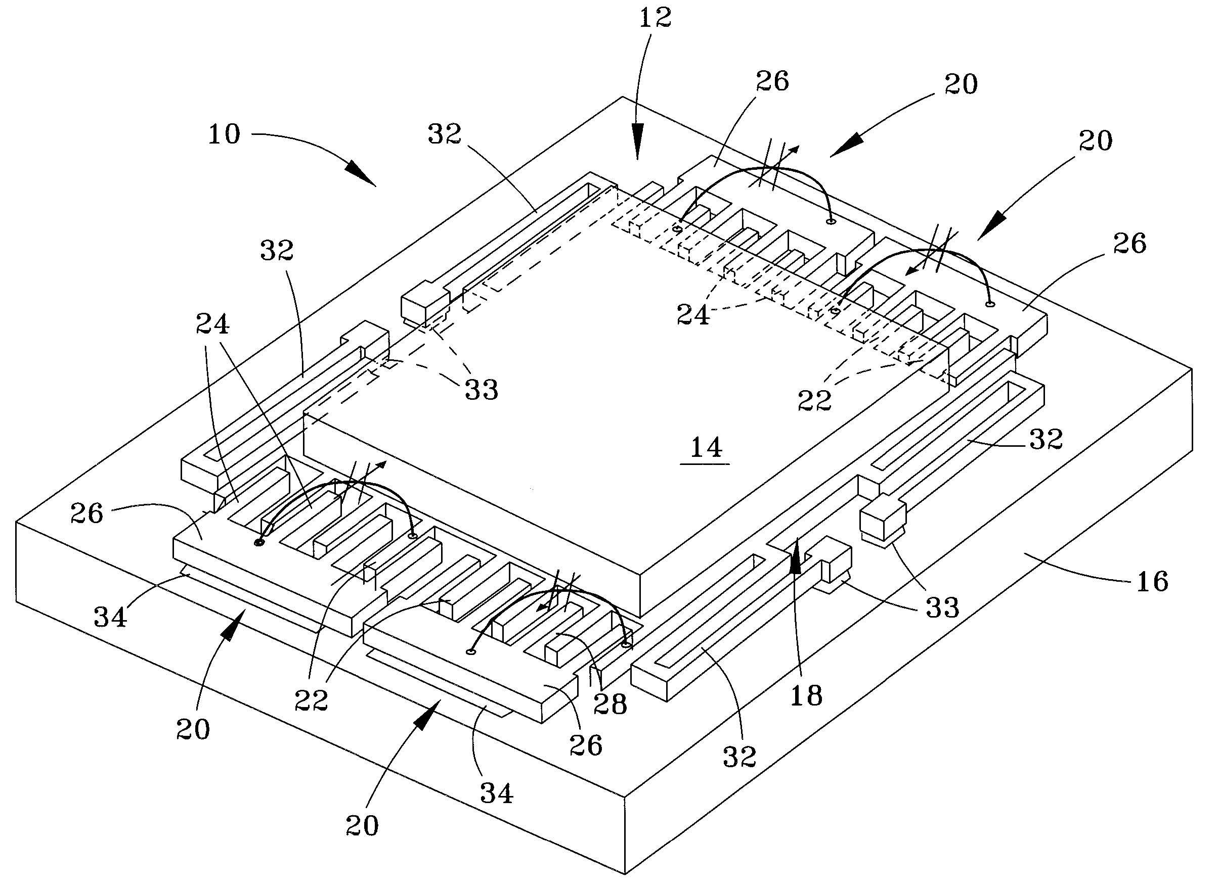
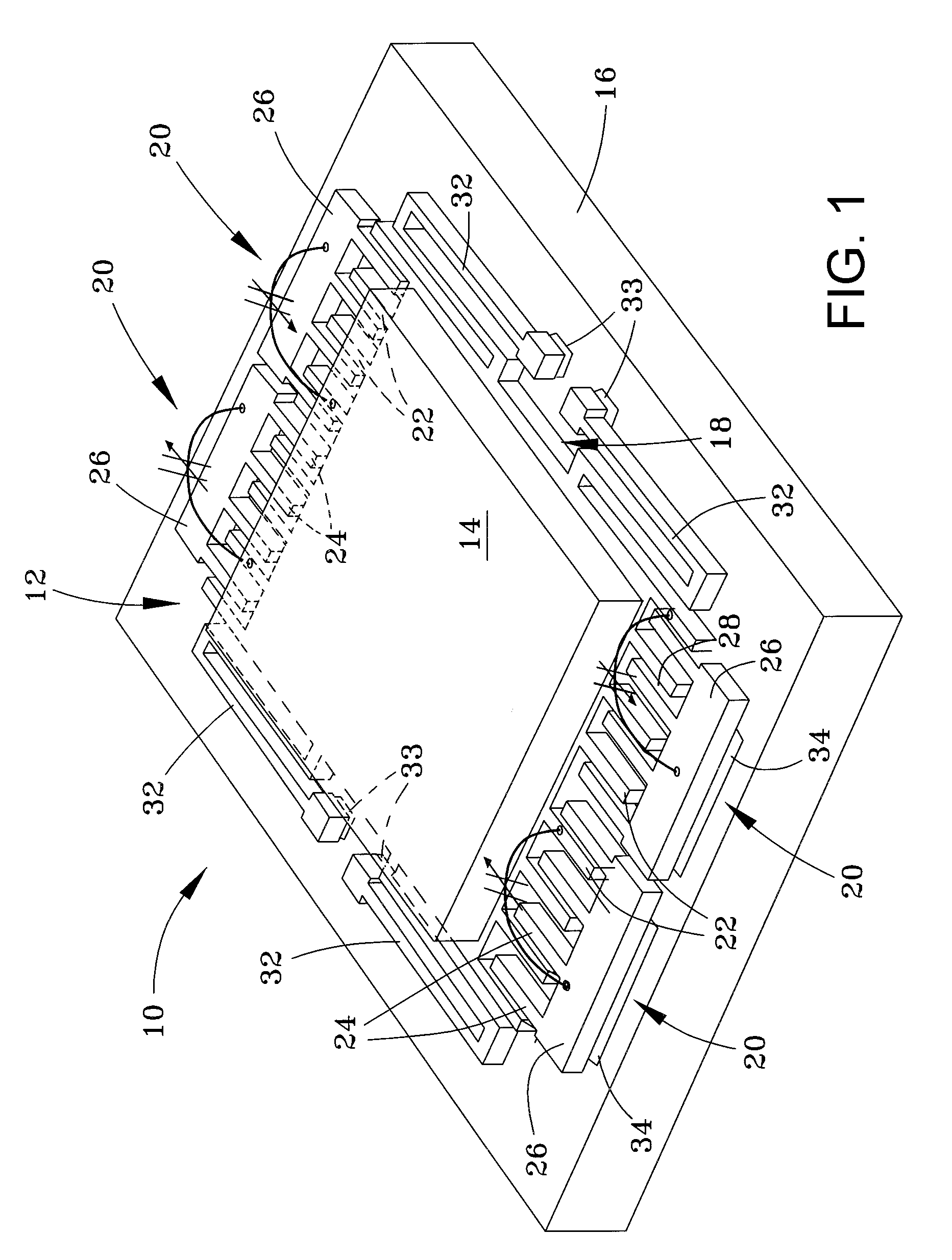
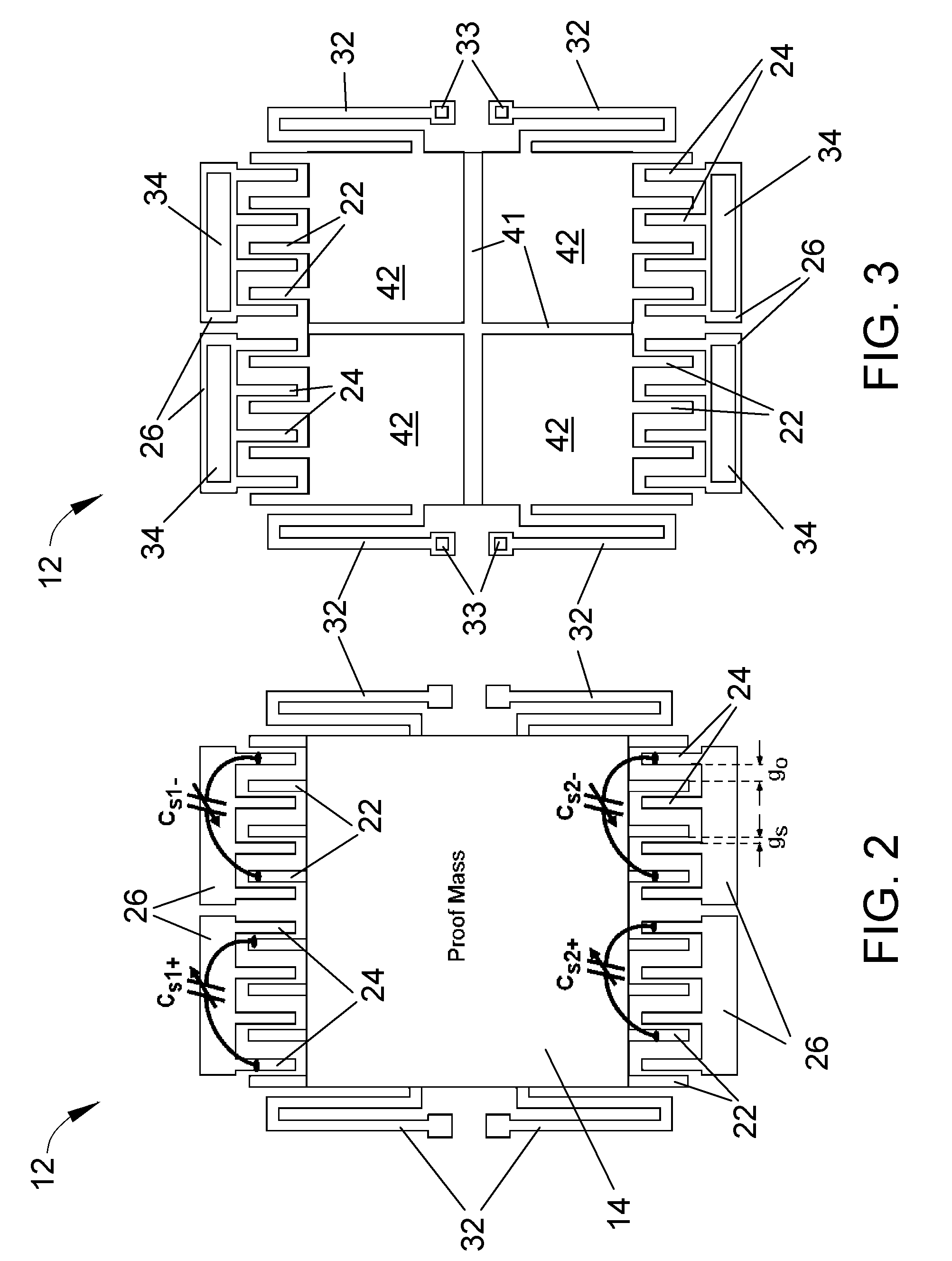
[0026]FIG. 1 is a perspective view of a sensor device 10 in accordance with an embodiment of the invention. As represented in FIG. 1, the sensor device 10 is a microelectromechanical system (MEMS) comprising a capacitive sensing element 12 supported above a substrate 16. Circuitry 18 (preferably CMOS interface circuitry) for the sensing element 12 is present on the substrate 16, preferably beneath the sensing element 12 as indicated in FIG. 1, though optionally on a surface region of the substrate 16 surrounding the element 12. The sensing element 12 includes a proof mass 14 with an in-plane axis of sensitivity, i.e., the plane of sensitivity is substantially parallel to the surface of the substrate 16. The sensing element 12 is preferably responsive to lateral motion or acceleration, though capacitive sensing for other purposes is also within the scope of this invention. As such, while the invention will be described with particular reference to a capacitive acceleration sensor dev...
PUM
 Abstract
Description
Claims
Application Information