

NAND Flash Memory with Densely Packed Memory Gates and Fabrication Process
a technology of memory gates and nand flash memory, which is applied in the direction of semiconductor devices, instruments, electrical equipment, etc., can solve the problems of difficult to form a high-voltage coupling ratio which is sufficient for program and erase operations, and is used in very high density data storage applications
- Summary
- Abstract
- Description
- Claims
- Application Information
AI Technical Summary
Benefits of technology
Problems solved by technology
Method used
Image

Examples
Embodiment Construction
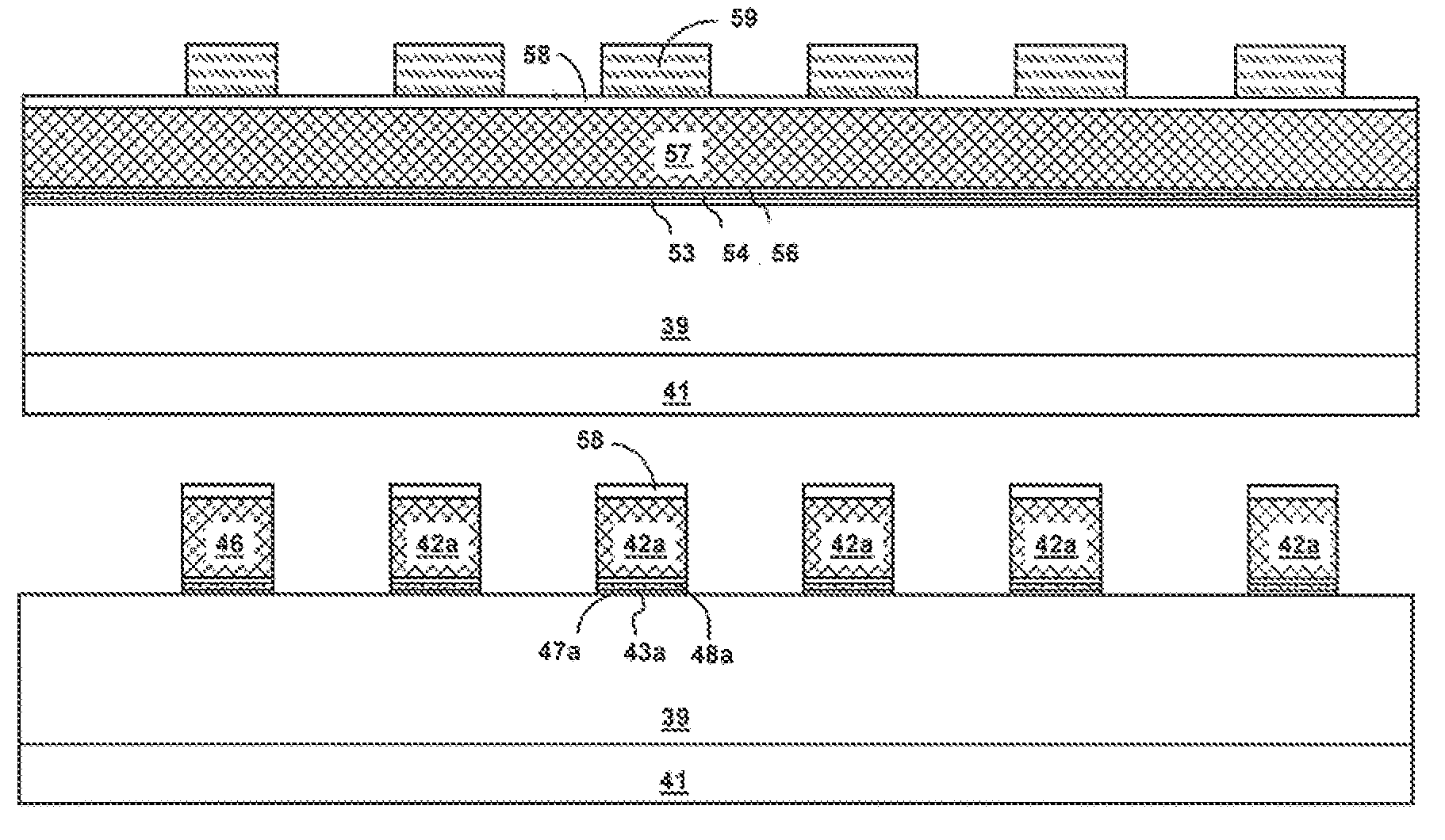
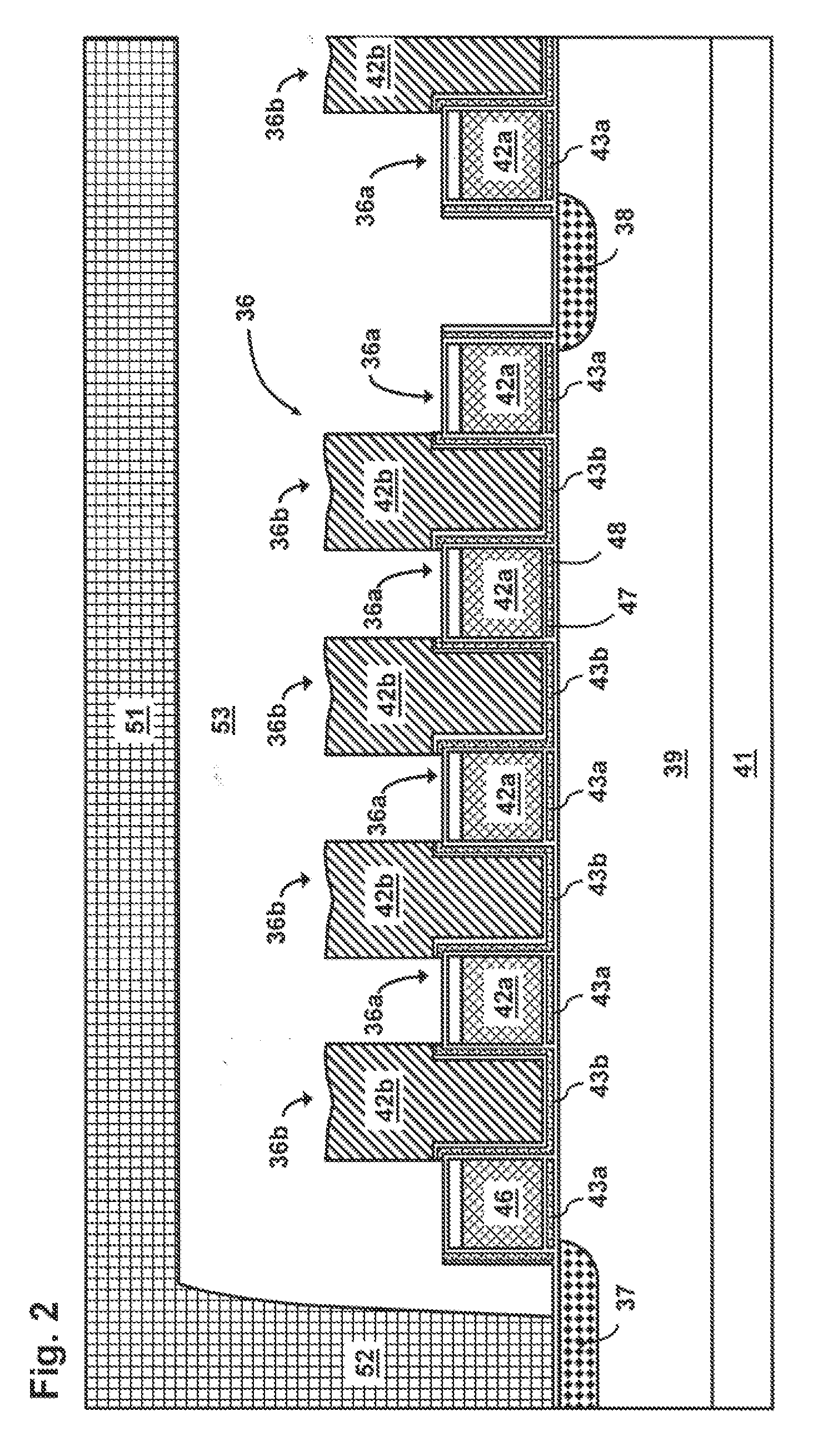
[0023] As illustrated in FIG. 2, the memory includes an array of NAND flash memory cells 36 which are arranged in rows between bit line diffusions 37 and a common source diffusion 38 formed in a P-type well 39 in the upper portion of a substrate 41 and doped with an N-type material. As discussed more fully hereinafter, in the preferred process of fabricating the cell array, the cells are formed in two groups 36a, 36b, with the cells in one group being interposed between the cells in the other. However, it will be understood that the array can be fabricated by other processes and that all of the cells can be formed in a single group.
[0024] The cells have memory or control gates 42a, 42b and charge storage gates 43a, 43b, with the control gates positioned above and aligned with the charge storage gates. A row select gate 46 is formed at the end of the row next to the bit line diffusion, with a passive (unused) charge storage gate 43a beneath it. The select gate partially overlaps the...
PUM
 Abstract
Description
Claims
Application Information