Organic thin film transistor and flat panel display device using the same
- Summary
- Abstract
- Description
- Claims
- Application Information
AI Technical Summary
Benefits of technology
Problems solved by technology
Method used
Image

Examples
first embodiment
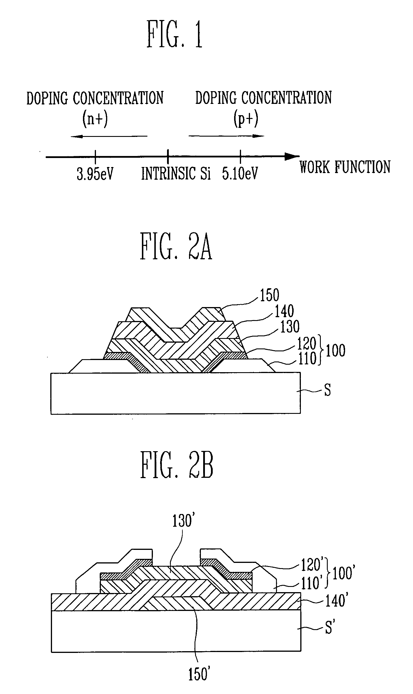
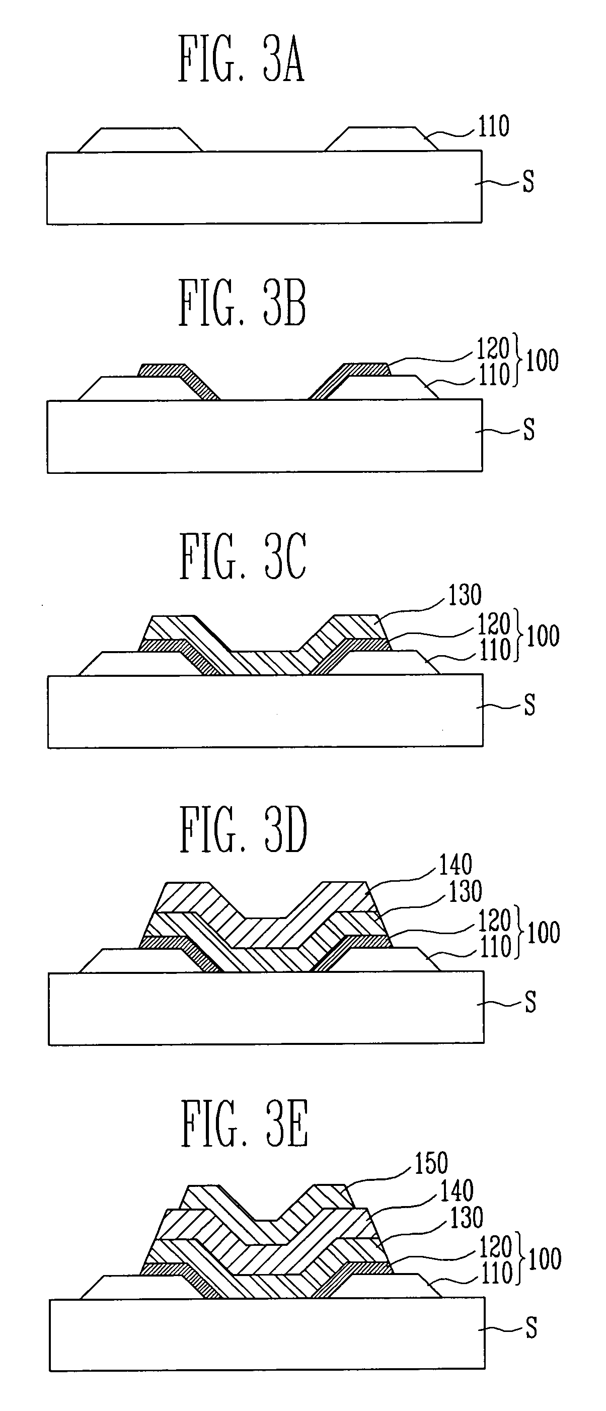
[0033] In a transistor having a p-type organic semiconductor layer (e.g., 130 or 130′) an inorganic layer (e.g., 120 or 120′) is doped to have a work function higher than a work function of the p-type organic semiconductor layer. In this case, referring also to FIG. 1, when silicon is used as the inorganic layer (or p-type semiconductor), the above-described condition can be satisfied by doping the silicon with a dopant density at more than 1018 / cm3 when the work function of the p-type semiconductor is 5.1 eV. For example, if the organic semiconductor layer contacting the source and drain electrodes is formed by pentacene and the inorganic layer forming the outer sides of the source and drain electrodes is formed by silicon, then the inorganic layer may be doped with boron at a dopant density of 1019 / cm3.
[0034] By contrast, in a transistor having an n-type organic semiconductor layer (e.g., 130 or 130′) according to the first embodiment of the present invention, an inorganic layer ...
second embodiment
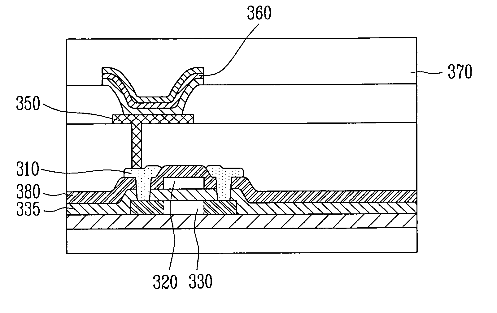
[0046]FIGS. 4A and 4B are schematic structural views illustrating an organic thin film transistor of a staggered structure and an organic thin film transistor of an inverted staggered structure according to the present invention.
[0047] As shown in FIGS. 4A and 4B, the organic thin film transistor is substantially the same as the organic thin film transistor employing the electrodes according to the first embodiment including the source / drain electrodes 200 (or 200′), an organic semiconductor layer 210 (or 210′), a gate insulator layer 220 (or 220′), and a gate electrode 230 (or 230′). However, the organic thin film transistor of FIGS. 4A and 4B is different from the organic thin film transistor of FIGS. 2A and 2B in that the source and drain electrodes 200 (or 200′) are formed by impurities doped-inorganic materials and contact the organic semiconductor layer 210 (or 210′). Thus, a detailed description of general components of the organic thin film transistor except for the source a...
PUM
 Abstract
Description
Claims
Application Information
 - R&D
- Intellectual Property
- Life Sciences
- Materials
- Tech Scout
- Unparalleled Data Quality
- Higher Quality Content
- 60% Fewer Hallucinations
Browse by: Latest US Patents, China's latest patents, Technical Efficacy Thesaurus, Application Domain, Technology Topic, Popular Technical Reports.
© 2025 PatSnap. All rights reserved.Legal|Privacy policy|Modern Slavery Act Transparency Statement|Sitemap|About US| Contact US: help@patsnap.com