

Floating-gate nonvolatile semiconductor memory device
- Summary
- Abstract
- Description
- Claims
- Application Information
AI Technical Summary
Benefits of technology
Problems solved by technology
Method used
Image

Examples
embodiment 1
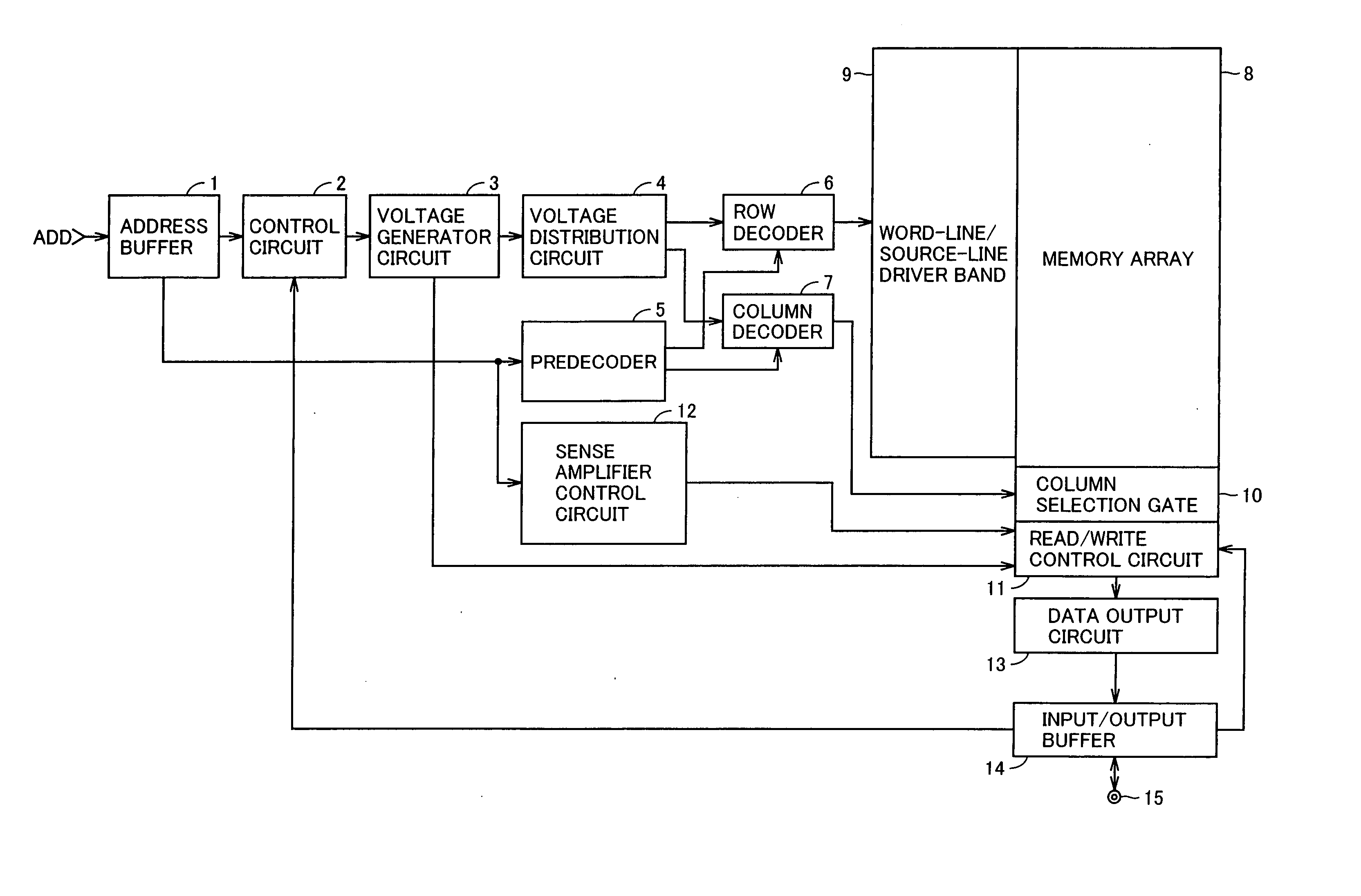
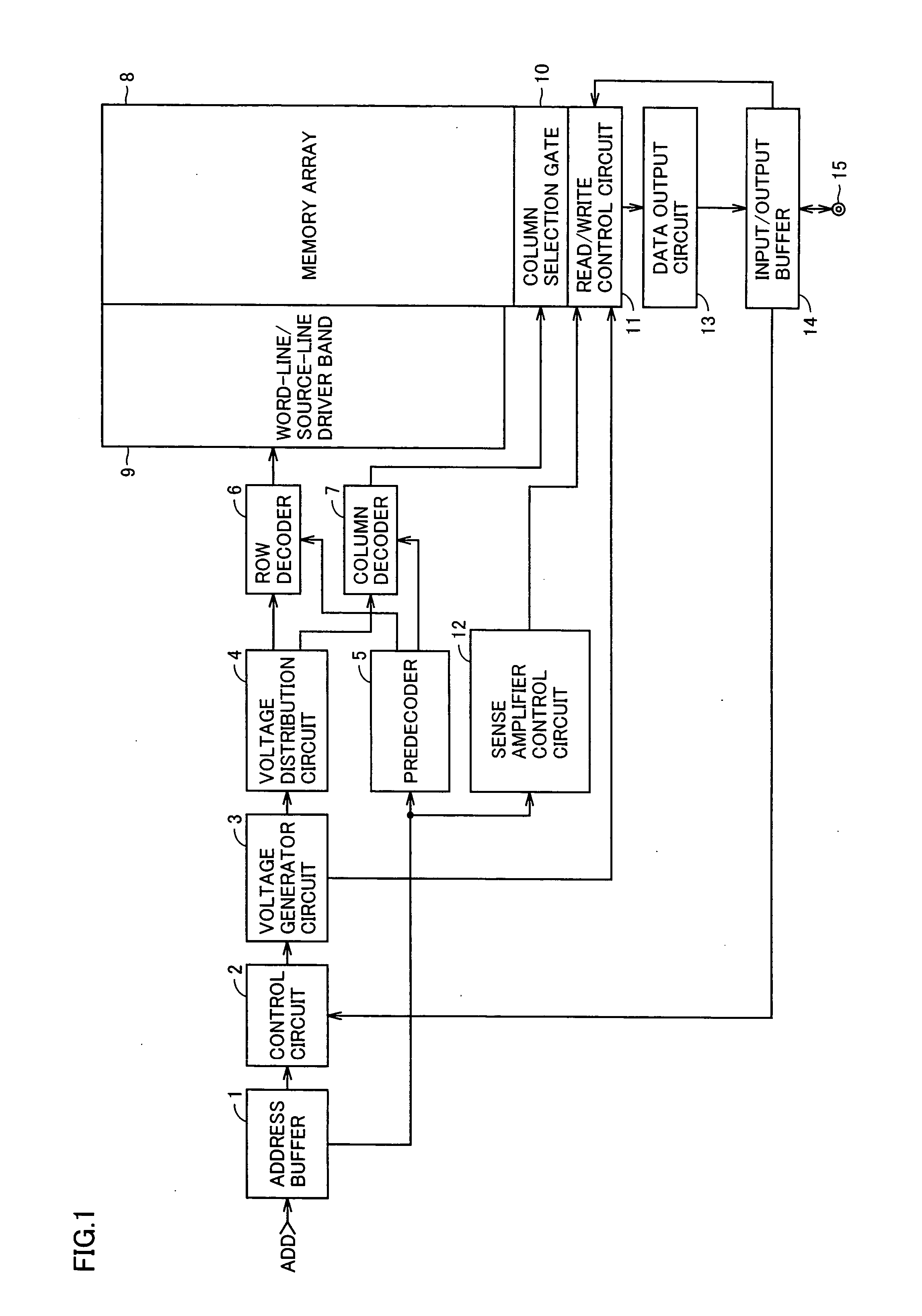
[0046]FIG. 1 is a block diagram showing the entire configuration of a nonvolatile semiconductor memory device according to an embodiment 1 of the present invention. In FIG. 1, the nonvolatile semiconductor memory device includes an address buffer 1 that receives an external address signal ADD and outputs an internal address signal, a control circuit 2 that receives the internal address signal from address buffer 1 and executes various kinds of operation controls, a voltage generator circuit 3 that generates a voltage used for each type of operation sequence based on the instruction from control circuit 2, and a voltage distribution circuit 4 that receives the voltage generated by voltage generator circuit 3 and adjusts the voltage level for distribution.
[0047] In addition, the nonvolatile semiconductor memory device has a predecoder 5 that receives the internal address signal from address buffer 1 and generates a predecoded row signal and a predecoded column signal, a row decoder 6...
modification example of embodiment 1
[0088]FIG. 18 is a flowchart showing an operation of a write sequence according to a modification example of the embodiment 1 of the present invention, which is to be compared with FIG. 10. FIG. 18 differs from FIG. 10 in that, in step S3, the sequence has a WAIT operation of a predetermined period of time, instead of applying the PGM detrapping pulse to the memory cell.
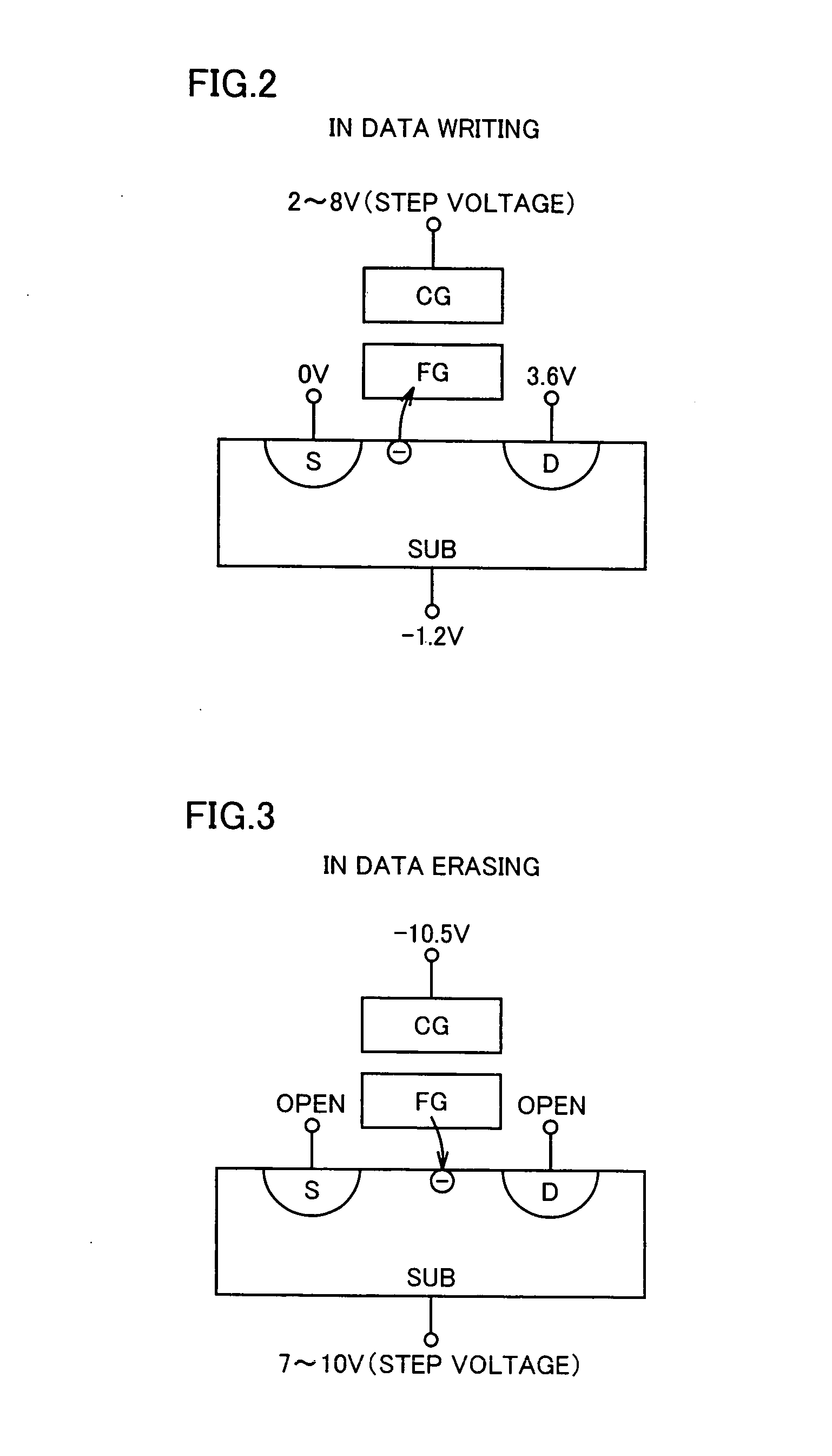
[0089]FIG. 19 is a cross-sectional view for illustrating a voltage applied to the memory cell during the WAIT operation in the write sequence shown in FIG. 18, which is to be compared with FIG. 11. FIG. 19 differs from FIG. 11 in that gate voltage VG applied to control gate CG is set at 0 V. After the WAIT state is kept for a predetermined period of time (on the order of μs to ms) with gate voltage VG, source voltage VS, drain voltage VD and substrate voltage VWELL all set at 0 V in this way, electrons trapped in oxide film OM or near the oxide film interface are automatically detrapped.
[0090]FIG. 20 is a time char...
embodiment 2
[0093]FIG. 23 is a flowchart showing a write sequence according to an embodiment 2 of the present invention, which is to be compared with FIG. 10. Steps S21, S22, S24 and S25 in FIG. 23 correspond to steps S1 to S4 in FIG. 10, respectively. In step S23, it is determined whether the number of program pulses applied to the memory cell has reached a predetermined number N. If the number of program pulses is less than N, the process proceeds to step S25 by skipping step S24, or if the number of program pulses is equal to or more than N, the process proceeds to step S24.
[0094] For example, if the number N is set at a half of the total number of program pulses, no PGM detrapping pulse is applied to the memory cell in the first half of the write sequence, and the PGM detrapping pulse is applied to the memory cell only in the latter half of the write sequence.
[0095]FIG. 24 is a time chart showing a temporal variation of gate voltage VG in the write sequence shown in FIG. 23, which is to b...
PUM
 Abstract
Description
Claims
Application Information